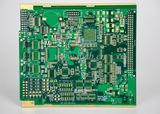
Min 3 Mil 0.1mm Hole High Density Interconnector Pcb For Industrial Control
-
High Light
3 mil high density interconnector pcb
,0.1mm hole high density interconnector pcb
,industrial control high density interconnect pcb
-
Product NameMin 3mil 0.1mm Hole High Density Interconnector PCB For Industrial Control
-
MaterialFR-4/Normal Tg/High Tg/Low Dk/HF FR4/PTEE/PI
-
Copper Thickness1oz ,2oz ...6oz
-
Min. Line Spacing0.030mm,0.05mm
-
Min. Hole Size0.05mm, 0.1mm, 0.25mm, 0.1mm/4mil, 4mil, 0.02
-
UsageCommunications, Industrial Control, Computer Applications, Aerospace, Military, Medical
-
Board Thickness1.6mm
-
Solder MaskGreen. Black. Red. Yellow. White. Blue Etc.; Custom
-
TypeBuried Vias And Through Vias
-
Surface FinishingENEPING /ENIG /HASL /FINGER GOLD/IMMERSION TIN/SELECTIVE THICK GOLD
-
Place of OriginCHINA
-
Brand NameHNL-PCBA
-
CertificationISO9001,IS16949, ISO14001,ROHS , UL, IPC-A , UL, QC080000
-
Model NumberPCB Assembly 012
-
Minimum Order Quantity1 PC
-
PriceNegotiable
-
Packaging DetailsESD packaging with carton box
-
Delivery Time1-7days
-
Payment TermsT/T, Western Union, L/C, MoneyGram
-
Supply Ability10,000,000 Point /Day
Min 3 Mil 0.1mm Hole High Density Interconnector Pcb For Industrial Control
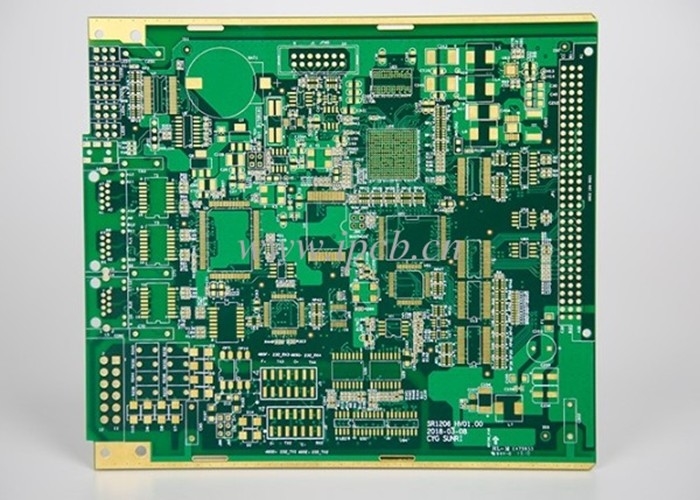
Min 3mil 0.1mm Hole High Density Interconnector PCB For Industrial Control
HDI PCB Board Introduction
Our products include: high-precision double-sided PCB circuit boards, PCB multilayer circuit boards, HDI circuit boards, PCB high-frequency boards, ceramic circuit boards and other special and difficult circuit boards, focusing on multi-variety, small and medium-sized batches.
PCB circuit boards are widely used in communications, industrial control, computer applications, aerospace, military, medical, testing equipment and other fields.
HDI is the abbreviation of High Density Interconnector, which is a (technology) for the production of printed circuit boards. HDI is a compact product designed for small volume users.
Advantages of HDI circuit
1. It can reduce the cost of PCB: when the density of the PCB increases beyond the eight-layer board, it is manufactured with HDI, and the cost will be lower than the traditional complex lamination process.
2. Increase line density: interconnection of traditional circuit boards and parts
3. Conducive to the use of advanced construction technology
4. Has better electrical performance and signal accuracy
5. Better reliability
6. Can improve thermal properties
7. Can improve radio frequency interference/electromagnetic wave interference/electrostatic discharge (RFI/EMI/ESD)
8. Increase design efficiency
PCB CAPABILITIES
| FACTORY CAPABILITIES | |||
| No. | Items | 2019 | 2020 |
| 1 | HDI Capabilities | HDI ELIC (4+2+4) | HDI ELIC(5+2+5) |
| 2 | Max layer count | 32L | 36L |
| 3 | Board Thickness | Core thickness 0.05mm-1.5mm ,Fineshed board thickness 0.3-3.5mm | Core thickness 0.05mm-1.5mm ,Fineshed board thickness 0.3-3.5mm |
| 4 | Min.Hole Size | Laser 0.075mm | Laser 0.05mm |
| Mechnical 0.15mm | Mechnical 0.15mm | ||
| 5 | Min Line Width/Space | 0.035mm/0.035mm | 0.030mm/0.030mm |
| 6 | Copper Thickness | 1/3oz-4oz | 1/3oz-6oz |
| 7 | Size Max Panel size | 700x610mm | 700x610mm |
| 8 | Registration Accuracy | +/-0.05mm | +/-0.05mm |
| 9 | Routing Accuracy | +/-0.075mm | +/-0.05mm |
| 10 | Min.BGA PAD | 0.15mm | 0.125mm |
| 11 | Max Aspect Ratio | 10:1 | 10:1 |
| 12 | Bow and Twist | 0.50% | 0.50% |
| 13 | Impedance Control Tolerance | +/-8% | +/-5% |
| 14 | Daily Output | 3,000m2 (Max capacity of equipment) | 4,000m2 (Max capacity of equipment) |
| 15 | Surface Finishing | ENEPING /ENIG /HASL /FINGER GOLD/IMMERSION TIN/SELECTIVE THICK GOLD | |
| 16 | Raw Material | FR-4/Normal Tg/High Tg/Low Dk/HF FR4/PTEE/PI | |
The types of HDI PCB
1.through vias from surface to surface,
2.with buried vias and through vias,
3.two or more HDI layer with through vias,
4.passive substrate with no electrical connection,
5.coreless construction using layer pairs
6.alternate constructions of coreless constructions using layer pairs.
HDI (High Density Interconnection) circuit boards usually include laser blind vias and mechanical blind vias; general through buried vias, blind vias, stacked vias, staggered vias, cross blind buried, through vias, blind via filling plating, fine line small gaps, The technology of realizing the conduction between the inner and outer layers by processes such as micro-holes in the disk, usually the diameter of the blind buried is not more than 6 mils.
![]()
Work flow for HDI
Board Cut - Inner Wet film -DES - AOI - Brown Oxido - Outer Layer Press - Out Layer Lamination - X-RAY & Rounting - Copper reduce & brown oxide - Laser Drilling - Drilling - Desmear PTH - Panel plating - Outer Layer dry film - Etching - AOI- Impedance Testing - S/M Pluged hole - Solder Mask - Component Mark - Impedance testing - Immersion Gold -V-cut - Routing - Electrical Test - FQC - FQA -Package -Shipment
![]()
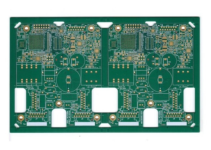
Similar products
![]()
HDI PCB Board Application Field
Our PCB are widely used in mobile phones, digital (camera) cameras, notebook computers, automotive electronics and other digital products, communication equipment, industrial control, consumer electronics, medical equipment, aerospace, light-emitting diode lighting, automotive electronics etc.
Workshop
![]()
![]()
![]()
Common packaging
1.PCB: Vacuum packaging with carton box
2.PCBA: ESD packaging with carton box
![]()
Our advantage
1.Service value
Independent quotation system to quickly serve the market
2.PCB manufacturing
High-tech PCB and PCB assembly production line
3.Material purchasing
A team of experienced electronic component procurement engineers
4.SMT post soldering
Dust-free workshop, high-end SMT patch processing
FAQ
Q1:What kind of PCB file format can you accept for production?
Gerber, PROTEL 99SE, PROTEL DXP, CAM350, ODB+(.TGZ)
Q2:Is my PCB files safe when I submit them to you for manufacturing?
We respect customer's copyright and will never manufacture PCB for someone else with your files unless we receive written permission from you, nor we'll share these files with any other 3rd parties.
Q3:What payments do you accept ?
-Telex Transfer(T/T),Western Union,Letter of Credit(L/C)
-Paypal,AliPay,Credit Card
Q4:How to get the PCB?
A:For small packages, we will ship the boards to you by DHL,UPS,FedEx,EMS. Door to door service! You will get your PCBs at your home.
B:For heavy goods more than 300kg, we may ship your boards by ship or by air to save freight cost. Of course, if you have your own forwarder, we may contact them for dealing with your shipment.
Q5:What is your minimum order quantity?
Our MOQ is 1 PCS.
Q6: Can we visit your company?
No problem. You are welcome to visit us in Beijing. Or the branch factory is in Tianjin.
Q7: How can you ensure the quality of the PCB?
Our PCBs are 100% test including Flying Probe Test, E-test and AOI.
![]()
Our services cover all industries and reach all parts of the world.