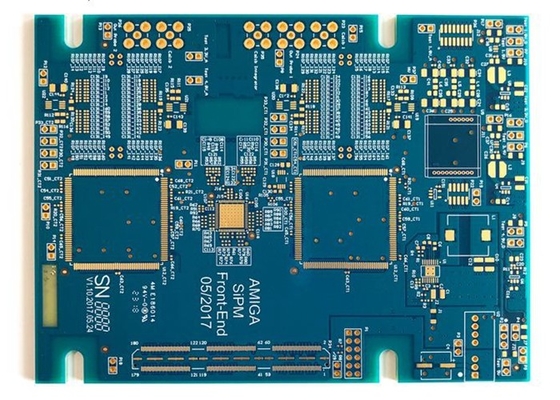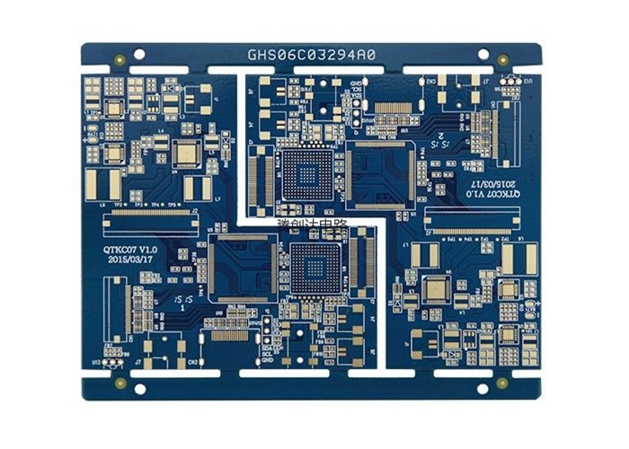
High Density Interconnection (HDI) PCB is a kind of (technology) for the production of printed circuit boards. It is a circuit board with relatively high circuit distribution density using micro blind via and buried via technology. Due to the continuous development of technology and the electrical requirements for high-speed signals, the circuit board must provide impedance control with AC characteristics, high-frequency transmission capability, and reduce unnecessary radiation (EMI). Adopting the structure of Stripline and Microstrip, multi-layering becomes a necessary design. In order to reduce the quality problem of signal transmission, insulating materials with low dielectric constant and low attenuation rate are used. In order to meet the miniaturization and arraying of electronic components, the density of circuit boards is constantly increasing to meet the demand.
PCB (Printed circuit board) is the most import role in the Electronic time, the electronic products which we can think of will need the PCB board, We are manufacture with year's experience in PCB & PCBA solutions .
PCB CAPABILITIES
| FACTORY CAPABILITIES | |||
| No. | Items | 2019 | 2020 |
| 1 | HDI Capabilities | HDI ELIC (4+2+4) | HDI ELIC(5+2+5) |
| 2 | Max layer count | 32L | 36L |
| 3 | Board Thickness | Core thickness 0.05mm-1.5mm ,Fineshed board thickness 0.3-3.5mm | Core thickness 0.05mm-1.5mm ,Fineshed board thickness 0.3-3.5mm |
| 4 | Min.Hole Size | Laser 0.075mm | Laser 0.05mm |
| Mechnical 0.15mm | Mechnical 0.15mm | ||
| 5 | Min Line Width/Space | 0.035mm/0.035mm | 0.030mm/0.030mm |
| 6 | Copper Thickness | 1/3oz-4oz | 1/3oz-6oz |
| 7 | Size Max Panel size | 700x610mm | 700x610mm |
| 8 | Registration Accuracy | +/-0.05mm | +/-0.05mm |
| 9 | Routing Accuracy | +/-0.075mm | +/-0.05mm |
| 10 | Min.BGA PAD | 0.15mm | 0.125mm |
| 11 | Max Aspect Ratio | 10:1 | 10:1 |
| 12 | Bow and Twist | 0.50% | 0.50% |
| 13 | Impedance Control Tolerance | +/-8% | +/-5% |
| 14 | Daily Output | 3,000m2 (Max capacity of equipment) | 4,000m2 (Max capacity of equipment) |
| 15 | Surface Finishing | ENEPING /ENIG /HASL /FINGER GOLD/IMMERSION TIN/SELECTIVE THICK GOLD | |
| 16 | Raw Material | FR-4/Normal Tg/High Tg/Low Dk/HF FR4/PTEE/PI | |
1.through vias from surface to surface,
2.with buried vias and through vias,
3.two or more HDI layer with through vias,
4.passive substrate with no electrical connection,
5.coreless construction using layer pairs
6.alternate constructions of coreless constructions using layer pairs.
HDI (High Density Interconnection) circuit boards usually include laser blind vias and mechanical blind vias; general through buried vias, blind vias, stacked vias, staggered vias, cross blind buried, through vias, blind via filling plating, fine line small gaps, The technology of realizing the conduction between the inner and outer layers by processes such as micro-holes in the disk, usually the diameter of the blind buried is not more than 6 mils.
![]()
Board Cut - Inner Wet film -DES - AOI - Brown Oxido - Outer Layer Press - Out Layer Lamination - X-RAY & Rounting - Copper reduce & brown oxide - Laser Drilling - Drilling - Desmear PTH - Panel plating - Outer Layer dry film - Etching - AOI- Impedance Testing - S/M Pluged hole - Solder Mask - Component Mark - Impedance testing - Immersion Gold -V-cut - Routing - Electrical Test - FQC - FQA -Package -Shipment
![]()
![]()
![]()
Our PCB are widely used in communication equipment, industrial control, consumer electronics, medical equipment, aerospace, light-emitting diode lighting, automotive electronics etc.
Workshop
![]()
![]()
![]()
1.PCB: Vacuum packaging with carton box
2.PCBA: ESD packaging with carton box
![]()
1.Service value
Independent quotation system to quickly serve the market
2.PCB manufacturing
High-tech PCB and PCB assembly production line
3.Material purchasing
A team of experienced electronic component procurement engineers
4.SMT post soldering
Dust-free workshop, high-end SMT patch processing
![]()
Our services cover all industries and reach all parts of the world.