Advantages of HDI circuit board
1. It can reduce the cost of PCB: when the density of the PCB increases beyond the eight-layer board, it is manufactured with HDI, and the cost will be lower than the traditional complex lamination process.
2. Increase line density: interconnection of traditional circuit boards and parts
3. Conducive to the use of advanced construction technology
4. Has better electrical performance and signal accuracy
5. Better reliability
6. Can improve thermal properties
7. Can improve radio frequency interference/electromagnetic wave interference/electrostatic discharge (RFI/EMI/ESD)
8. Increase design efficiency
HDI is the abbreviation of High Density Interconnector, which is a (technology) for the production of printed circuit boards. HDI is a compact product designed for small volume users.
PCB CAPABILITIES
| FACTORY CAPABILITIES | |||
| No. | Items | 2019 | 2020 |
| 1 | HDI Capabilities | HDI ELIC (4+2+4) | HDI ELIC(5+2+5) |
| 2 | Max layer count | 32L | 36L |
| 3 | Board Thickness | Core thickness 0.05mm-1.5mm ,Fineshed board thickness 0.3-3.5mm | Core thickness 0.05mm-1.5mm ,Fineshed board thickness 0.3-3.5mm |
| 4 | Min.Hole Size | Laser 0.075mm | Laser 0.05mm |
| Mechnical 0.15mm | Mechnical 0.15mm | ||
| 5 | Min Line Width/Space | 0.035mm/0.035mm | 0.030mm/0.030mm |
| 6 | Copper Thickness | 1/3oz-4oz | 1/3oz-6oz |
| 7 | Size Max Panel size | 700x610mm | 700x610mm |
| 8 | Registration Accuracy | +/-0.05mm | +/-0.05mm |
| 9 | Routing Accuracy | +/-0.075mm | +/-0.05mm |
| 10 | Min.BGA PAD | 0.15mm | 0.125mm |
| 11 | Max Aspect Ratio | 10:1 | 10:1 |
| 12 | Bow and Twist | 0.50% | 0.50% |
| 13 | Impedance Control Tolerance | +/-8% | +/-5% |
| 14 | Daily Output | 3,000m2 (Max capacity of equipment) | 4,000m2 (Max capacity of equipment) |
| 15 | Surface Finishing | ENEPING /ENIG /HASL /FINGER GOLD/IMMERSION TIN/SELECTIVE THICK GOLD | |
| 16 | Raw Material | FR-4/Normal Tg/High Tg/Low Dk/HF FR4/PTEE/PI | |
1.through vias from surface to surface,
2.with buried vias and through vias,
3.two or more HDI layer with through vias,
4.passive substrate with no electrical connection,
5.coreless construction using layer pairs
6.alternate constructions of coreless constructions using layer pairs.
HDI (High Density Interconnection) circuit boards usually include laser blind vias and mechanical blind vias; general through buried vias, blind vias, stacked vias, staggered vias, cross blind buried, through vias, blind via filling plating, fine line small gaps, The technology of realizing the conduction between the inner and outer layers by processes such as micro-holes in the disk, usually the diameter of the blind buried is not more than 6 mils.
![]()
Board Cut - Inner Wet film -DES - AOI - Brown Oxido - Outer Layer Press - Out Layer Lamination - X-RAY & Rounting - Copper reduce & brown oxide - Laser Drilling - Drilling - Desmear PTH - Panel plating - Outer Layer dry film - Etching - AOI- Impedance Testing - S/M Pluged hole - Solder Mask - Component Mark - Impedance testing - Immersion Gold -V-cut - Routing - Electrical Test - FQC - FQA -Package -Shipment
![]()
![]()
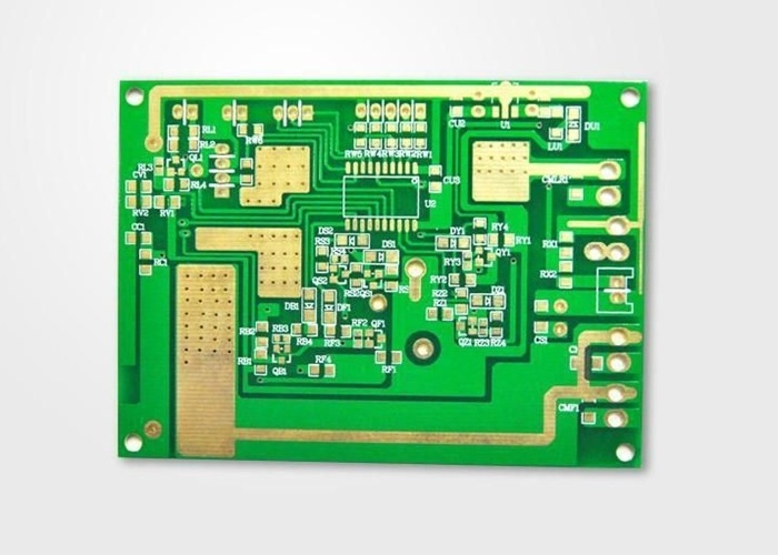
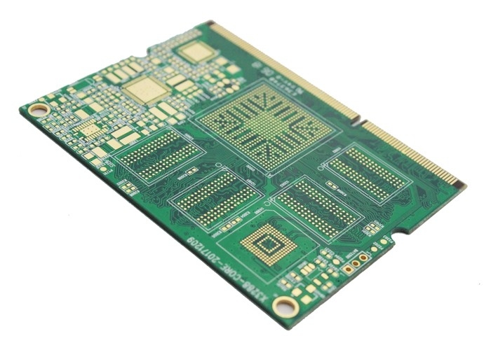
Our PCB are widely used in mobile phones, digital (camera) cameras, notebook computers, automotive electronics and other digital products, communication equipment, industrial control, consumer electronics, medical equipment, aerospace, light-emitting diode lighting, automotive electronics etc.
Workshop
![]()
![]()
![]()
1.PCB: Vacuum packaging with carton box
2.PCBA: ESD packaging with carton box
![]()
1.Service value
Independent quotation system to quickly serve the market
2.PCB manufacturing
High-tech PCB and PCB assembly production line
3.Material purchasing
A team of experienced electronic component procurement engineers
4.SMT post soldering
Dust-free workshop, high-end SMT patch processing
![]()
We have profuse experience in manufacturing PCB,owned experienced technical R & D technology team, young and professional sales and customer service team, experienced and professional procurement team and assembly testing team, which make sure the products quality of the pass rate, on-time delivery rate of customer orders.
Our services include: circuit board design and layout, 2-46 layers PCB manufacturing, professional FPC production, electronic components purchasing, SMT professional processing, Soldering and Assembly, especially sample and small bulk orders. we have the advantages of a quick quote, fast production, fast delivery.
Our services cover all industries and reach all parts of the world.