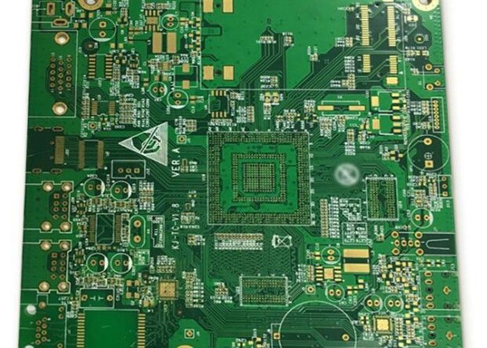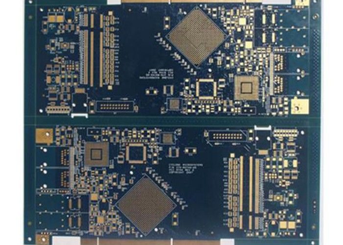
HDI PCB is a special type of PCB, and it has the capability of high-density interconnections. In other words, it has more wires or conduction lines per unit area, utilizing the most of the space & offering a compact PCB. But the board functionally isn’t affected.
HDI Board contains blind and buried vias and often contain microvias of 0.006 or less in diameter.
HDI board has higher circuitry density than traditional circuit boards.
All of the other electronic components are mounted on the printed circuit boards(PCBs),which are the foundation.
PCBs have mechanical and electrical attributes,making them for ideal applications. Most PCB’s fabricated are rigid, roughly 90% of the PCB’s manufactured today are rigid boards.
| FACTORY CAPABILITIES | |||
| No. | Items | 2019 | 2020 |
| 1 | HDI Capabilities | HDI ELIC (4+2+4) | HDI ELIC(5+2+5) |
| 2 | Max layer count | 32L | 36L |
| 3 | Board Thickness | Core thickness 0.05mm-1.5mm ,Fineshed board thickness 0.3-3.5mm | Core thickness 0.05mm-1.5mm ,Fineshed board thickness 0.3-3.5mm |
| 4 | Min.Hole Size | Laser 0.075mm | Laser 0.05mm |
| Mechnical 0.15mm | Mechnical 0.15mm | ||
| 5 | Min Line Width/Space | 0.035mm/0.035mm | 0.030mm/0.030mm |
| 6 | Copper Thickness | 1/3oz-4oz | 1/3oz-6oz |
| 7 | Size Max Panel size | 700x610mm | 700x610mm |
| 8 | Registration Accuracy | +/-0.05mm | +/-0.05mm |
| 9 | Routing Accuracy | +/-0.075mm | +/-0.05mm |
| 10 | Min.BGA PAD | 0.15mm | 0.125mm |
| 11 | Max Aspect Ratio | 10:1 | 10:1 |
| 12 | Bow and Twist | 0.50% | 0.50% |
| 13 | Impedance Control Tolerance | +/-8% | +/-5% |
| 14 | Daily Output | 3,000m2 (Max capacity of equipment) | 4,000m2 (Max capacity of equipment) |
| 15 | Surface Finishing | ENEPING /ENIG /HASL /FINGER GOLD/IMMERSION TIN/SELECTIVE THICK GOLD | |
| 16 | Raw Material | FR-4/Normal Tg/High Tg/Low Dk/HF FR4/PTEE/PI | |
1.through vias from surface to surface,
2.with buried vias and through vias,
3.two or more HDI layer with through vias,
4.passive substrate with no electrical connection,
5.coreless construction using layer pairs
6.alternate constructions of coreless constructions using layer pairs.
![]()
Board Cut - Inner Wet film -DES - AOI - Brown Oxido - Outer Layer Press - Out Layer Lamination - X-RAY & Rounting - Copper reduce & brown oxide - Laser Drilling - Drilling - Desmear PTH - Panel plating - Outer Layer dry film - Etching - AOI- Impedance Testing - S/M Pluged hole - Solder Mask - Component Mark - Impedance testing - Immersion Gold -V-cut - Routing - Electrical Test - FQC - FQA -Package -Shipment
![]()
PCB Assembly Process
![]()
![]()
![]()
| Product Type | Qty | Normal lead time | Quick-turn lead time |
| SMT+DIP | 1-50 | 1WD-2WD | 8H |
| SMT+DIP | 51-200 | 2WD-3WD | 1.5WD |
| SMT+DIP | 201-2000 | 3WD-4WD | 2WD |
| SMT+DIP | ≥2001 | 4WD-5WD | 3WD |
| PCBA(2-4Layer) | 1-50 | 2.5WD-3.5WD | 1WD |
| PCBA(2-4Layer) | 51-2000 | 5WD-6WD | 2.5WD |
| PCBA(2-4Layer) | ≥2001 | ≥7WD | 5WD |
| PCBA(6-10Layer) | 1-50 | 3WD-4WD | 2.5WD |
| PCBA(6-10Layer) | 51-2000 | 7WD-8WD | 6WD |
| PCBA(10-HDILayer) | 1-50 | 7WD-9WD | 5WD |
| PCBA(10-HDILayer) | 51-2000 | 9WD-11WD | 7WD |
Our products are widely used in communication equipment, industrial control, consumer electronics, medical equipment, aerospace, light-emitting diode lighting, automotive electronics etc.
![]()
Workshop
![]()
![]()
![]()
1.PCB: Vacuum packaging with carton box
2.PCBA: ESD packaging with carton box
![]()
1.Service value
Independent quotation system to quickly serve the market
2.PCB manufacturing
High-tech PCB and PCB assembly production line
3.Material purchasing
A team of experienced electronic component procurement engineers
4.SMT post soldering
Dust-free workshop, high-end SMT patch processing
![]()
Our services cover all industries and reach all parts of the world.