
Haina lean Electronics Co., Ltd is one of the most professional PCB manufacture in Beijing,China.With 10 years of development, Haina Lean Electronics turns into a first class manufacture of HDI PCB , and undertake various board PCB services, including 1-36, HDI, thick copper layer, rigid flex, high frequency, Rogers+FR-4 mixed medium volume, lamination, buried aluminum, copper substrate, plate making proofing or quick expedited PCB proofing.
| No. | Items | |
| 1 | HDI Capabilities | HDI ELIC(5+2+5) |
| 2 | Max layer count | 36L |
| 3 | Board Thickness | Core thickness 0.05mm-1.5mm ,Fineshed board thickness0.3-3.5mm |
| 4 | Min.Hole Size | Laser 0.05mm |
| Mechnical 0.15 | ||
| 5 | Min Line Width/Space | 0.030mm/0.030mm |
| 6 | Copper Thickness | 1/3oz-6oz |
| 7 | Size Max Panel size | 700x610mm |
| 8 | Registration Accuracy | +/-0.05mm |
| 9 | Routing Accuracy | +/-0.05mm |
| 10 | Min.BGA PAD | 0.125mm |
| 11 | Max Aspect Ratio | 10:01 |
| 12 | Bow and Twist | 0.50% |
| 13 | Impedance Control Tolerance | +/-5% |
| 14 | Daily output | 4,000m2 (Max capacity of equipment) |
| 15 | Surface Finishing | ENEPING /ENIG /HASL /FINGER GOLD/IMMERSION TIN/SELECTIVE THICK GOLD |
| 16 | Raw Material | FR-4/Normal Tg/High Tg/Low Dk/HF FR4/PTEE/PI |
| PCBA Capability | |||
| Material Type | Item | Min | Max |
| PCB | Dimension (length,width,height.mm) | 50*40*0.38 | 600*400*4.2 |
| Material | FR-4,CEM-1,CEM-3,Aluminium-based board,Rogers,ceramic plate,FPC | ||
| Surface finish | HASL,OSP,Immersion gold,Flash Gold Finger | ||
| Components | Chip&IC | 1005 | 55mm |
| BGA Pitch | 0.3mm | - | |
| QFP Pitch | 0.3mm | - | |
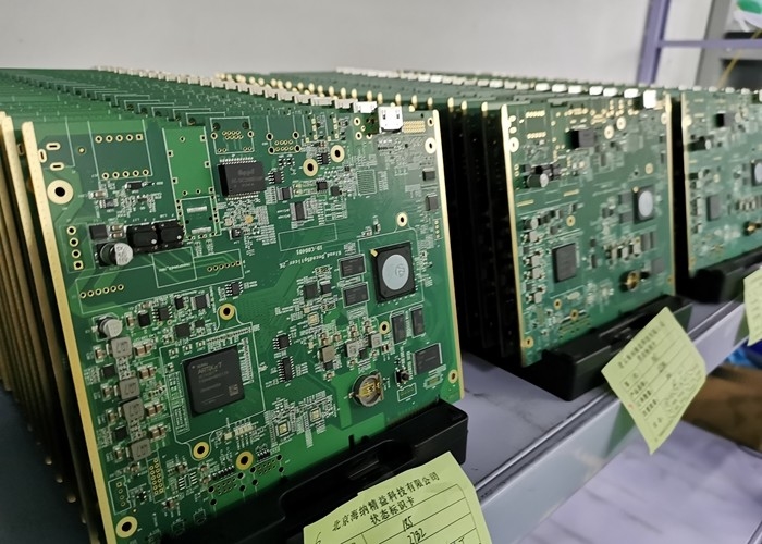
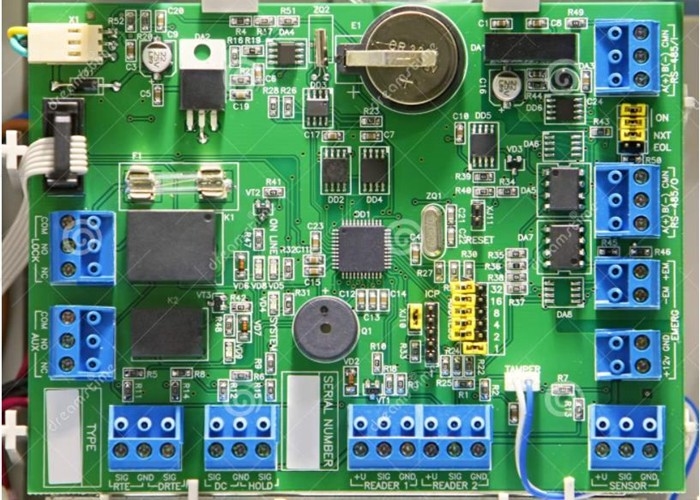
FR4 PCB Craftsmanship
Immersion gold ,Lead-free HASL,OSP,etc.
![]()
![]()
Our service
| Electronic Manufacturing Service | PCB Electronic Design |
| PCB Electronic Design | PCB Layout Service |
| PCB Assembly process service | PCBA Components Sourcing |
![]()
| Prototype PCB | Batch | Prototype | Expedited |
| Double sides | 9 Days | 5 Days | 45h |
| Four-layer | 10 Days | 5 Days | 3 Days |
| Six-layer | 12 Days | 6 Days | 3 Days |
| Eight-layer | 12 Days | 7 Days | 4 Days |
| Ten-layer | 14 Days | 10 Days | 4Days |
| Twelve-layer | 14 Days | 10 Days | 5 Days |
| Fourteen-layer | 16 Days | 12Days | 6 Days |
| Sixteen-layer | 16 Days | 12 Days | 6 Days |
| Eighteen-layer | 18 Days | 14 Days | 6 Days |
| Twenty-layer | 18 Days | 14 Days | 10 Days |
| Twenty two-layer | 20 Days | 14 Days | 10 Days |
| Twenty four-layer | 20 Days | 14 Days | 10 Days |
| Twenty six-layer | 20 Days | 14 Days | 10 Days |
| Twenty eight-layer | 20 Days | 14 Days | 10 Days |
FR4 Printed Circuit Board Application Field
Printed circuit boards And PCB Assembly are mainly used for many communication industry, medical equipments, consumer electronics ,automotive electronics , audio and video, optoelectronics, robotics, hydroelectric power, aerospace, education, power supply, printer ,Auto Industry ,Smart Home.etc.
![]()
![]()
![]()
![]()
![]()
Testing service
1. Manual visual inspection of PCB board
2. PCB board online test
3. PCB board function test
4. AOI (Automatic optical inspection)
5. Automatic X-ray inspection
6. Laser detection system
7. Size detection
Above is the PCB testing service.
Partners
![]()
PCB: Vacuum packaging with carton box
PCBA: ESD packaging with carton box
![]()
Our services cover all industries and reach all parts of the world.