Haina Lean technology is a leading PCB assembly manufacturing service located in Beijing ,China.
We provide complete turnkey solutions and fast turnaround of commissioned assembly, and we can deliver small batches to large batches on time.
Advanced automated placement machines and an excellent technical team can speed up the delivery speed and provide the best quality.
100% lead-free operation and RoHS compliant.
We focus on PCB manufacturing services in telecommunications, medical, driverless, military engineering, industrial control and other industries.
| FACTORY CAPABILITIES | |||
| No. | Items | 2019 | 2020 |
| 1 | HDI Capabilities | HDI ELIC (4+2+4) | HDI ELIC(5+2+5) |
| 2 | Max layer count | 32L | 36L |
| 3 | Board Thickness | Core thickness 0.05mm-1.5mm ,Fineshed board thickness 0.3-3.5mm | Core thickness 0.05mm-1.5mm ,Fineshed board thickness 0.3-3.5mm |
| 4 | Min.Hole Size | Laser 0.075mm | Laser 0.05mm |
| Mechnical 0.15 | Mechnical 0.15 | ||
| 5 | Min Line Width/Space | 0.035mm/0.035 | 0.030mm/0.030mm |
| 6 | Copper Thickness | 1/3oz-4oz | 1/3oz-6oz |
| 7 | Size Max Panel size | 700x610mm | 700x610mm |
| 8 | Registration Accuracy | +/-0.05mm | +/-0.05mm |
| 9 | Routing Accuracy | +/-0.075mm | +/-0.05mm |
| 10 | Min.BGA PAD | 0.15mm | 0.125mm |
| 11 | Max Aspect Ratio | 10:01 | 10:01 |
| 12 | Bow and Twist | 0.50% | 0.50% |
| 13 | Impedance Control Tolerance | +/-8% | +/-5% |
| 14 | Daily output | 3,000m2 (Max capacity of equipment) | 4,000m2 (Max capacity of equipment) |
| 15 | Surface Finishing | HASL Lead Free /ENEPING /ENIG /HASL /FINGER GOLD/IMMERSION TIN/SELECTIVE THICK GOLD | |
| 16 | Raw Material | FR-4/Normal Tg/High Tg/Low Dk/HF FR4/PTEE/PI | |
PCBA CAPABILITIES
| PCBA Capability | |||
| Material Type | Item | Min | Max |
| PCB | Dimension (length,width,height.mm) | 50*40*0.38 | 600*400*4.2 |
| Material | FR-4,CEM-1,CEM-3,Aluminium-based board,Rogers,ceramic plate,FPC | ||
| Surface finish | HASL,OSP,Immersion gold,Flash Gold Finger | ||
| Components | Chip&IC | 1005 | 55mm |
| BGA Pitch | 0.3mm | - | |
| QFP Pitch | 0.3mm | - | |
Drilling---Exposure---Plating---Etaching & Stripping---Punching---Electrical Testing---SMT--Wave Soldering---Assembling---ICT--Function Testing---Temperature & Humidity Testing
![]()
![]()
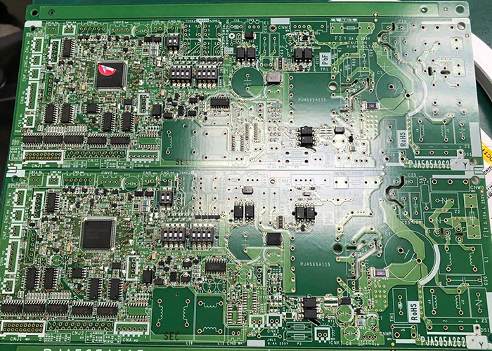
Printed circuit boards And PCB Assembly are mainly used for many communication industry ,Aprospace ,Auto Industry ,Communication,Indutrial Control ,Medical device ,Smart Home,consumer electronics ,automotive electronics , audio and video, optoelectronics, robotics, hydroelectric power, aerospace, education, power supply, printer ,Auto Industry ,Smart Home.etc.
![]()
![]()
![]()
1.PCB: Vacuum packaging with carton box
2.PCBA: ESD packaging with carton box
![]()
FAQ
Q1.What are needed for quoation ?
PCB :Gerber File (Protel.Power PCB ,PADs File)
PCBA: Gerber File and BOM
Q2. What file formats do you accept for production?
A: Gerber file: CAM350 RS274X
PCB file: Protel 99SE, P-CAD 2001 PCB
BOM: Excel (PDF,word,txt)
Q3.Are my files safe ?
Your files are held in complete safety and security ,we protect the intellectual property for our customers in the whole process .All documents from customer are never shared with any third parties .
Q4.What's your MOQ ?
No Moq ,We accept small orders as well as mass production
Q5.Shipping Cost ?
The shipping cost is determined by the destination ,weight ,packing size of the goods .We can provide shipping, air, land, express and other transportation services .
Q6.Can You provide fast rotating PCB ?
Yes , we can provide fast service 24 hours .
Q7.What are the services you can provide ?
One-stop contract manufacturing
A:PCB Assembly;
B:PCB Design & Layout
C:PCBA programming & functional testing;
D:Electronic components purchasing service;
E:Enclosure molding & final assembly with labels,instructions,enclosure, boxes.
Q8.Whether all PCBA s will be tested before delivery ?
Yes , we will test each piece of PCBA product under your testing methods ,to ensure quality and functionality .
Q9.Do you provide OEM service ?
Yes ,we offer PCB and PCBA OEM Service , we manufacture the PCB and PCBA products to your design and requirements .
Q10. Do you accept process materials supplied by clients?
A Yes, we can provide component source, and we also accept component from client
Haina lean Electronics Co., Ltd is a one-stop EMS supplier integrating PCB design, PCB manufacturing, Component sourcing and PCB assembly.
Here is strong component supply chain and procceurement team. Prototype and mass production are available. Competitive price is for high-quality and services. Exported to worldwide customer in US, Europe, Canada.
![]()
Our services cover all industries and reach all parts of the world.