Lead is the most comprehensive substance because it plays a fundamental & key role in electronic plating. Components used in lead-free PCB assembly should meet the requirements of lead-free compliance to ensure the reliability and suitability of final products. With more than 15 years' experience, Haina Lean Technology has maintained long-term cooperation relationship between renowned component manufacturers and distributors around the world, and we can purchase high quality lead-free components for our customers and care the environmental concerns.
PCBA CAPABILITIES
| FACTORY CAPABILITIES | |||
| No. | Items | 2020 | |
| 1 | HDI Capabilities | HDI ELIC(5+2+5) | |
| 2 | Max layer count | 46L | |
| 3 | Board Thickness | Core thickness 0.05mm-1.5mm ,Fineshed board thickness 0.3-3.5mm | |
| 4 | Min.Hole Size | Laser 0.05mm | |
| Mechnical 0.15 | |||
| 5 | Min Line Width/Space | 0.030mm/0.030mm | |
| 6 | Copper Thickness | 1/3oz-6oz | |
| 7 | Size Max Panel size | 700x610mm | |
| 8 | Registration Accuracy | +/-0.05mm | |
| 9 | Routing Accuracy | +/-0.05mm | |
| 10 | Min.BGA PAD | 0.125mm | |
| 11 | Max Aspect Ratio | 10:01 | |
| 12 | Bow and Twist | 0.50% | |
| 13 | Impedance Control Tolerance | +/-5% | |
| 14 | Daily output | 4,000m2 (Max capacity of equipment) | |
| 15 | Surface Finishing | HASL Lead Free /ENEPING /ENIG /HASL /FINGER GOLD/IMMERSION TIN/SELECTIVE THICK GOLD | |
| 16 | Raw Material | FR-4/Normal Tg/High Tg/Low Dk/HF FR4/PTEE/PI | |
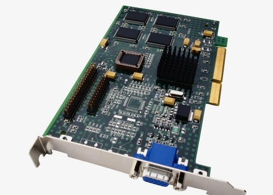
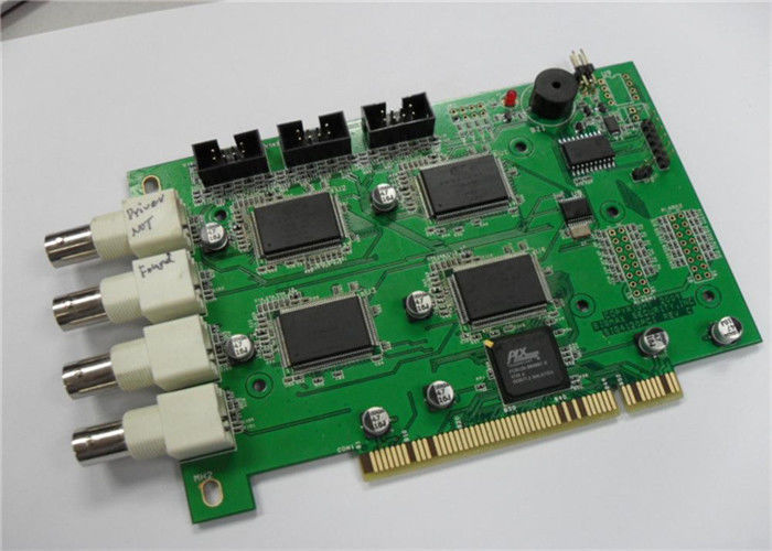
PCB assembly process
Drilling---Exposure---Plating---Etaching & Stripping---Punching---Electrical Testing---SMT--Wave Soldering---Assembling---ICT--Function Testing---Temperature & Humidity Testing
![]()
![]()
| Product Type | Qty | Normal lead time | Quick-turn lead time |
| SMT+DIP | 1-50 | 1WD-2WD | 8H |
| SMT+DIP | 51-200 | 2WD-3WD | 1.5WD |
| SMT+DIP | 201-2000 | 3WD-4WD | 2WD |
| SMT+DIP | ≥2001 | 4WD-5WD | 3WD |
| PCBA(2-4Layer) | 1-50 | 2.5WD-3.5WD | 1WD |
| PCBA(2-4Layer) | 51-2000 | 5WD-6WD | 2.5WD |
| PCBA(2-4Layer) | ≥2001 | ≥7WD | 5WD |
| PCBA(6-10Layer) | 1-50 | 3WD-4WD | 2.5WD |
| PCBA(6-10Layer) | 51-2000 | 7WD-8WD | 6WD |
| PCBA(10-HDILayer) | 1-50 | 7WD-9WD | 5WD |
| PCBA(10-HDILayer) | 51-2000 | 9WD-11WD | 7WD |
Printed circuit boards And PCB Assembly are mainly used for many communication industry ,Aprospace ,Auto Industry ,Communication,Indutrial Control ,Medical device ,Smart Home,consumer electronics ,automotive electronics , audio and video, optoelectronics, robotics, hydroelectric power, aerospace, education, power supply, printer ,Auto Industry ,Smart Home.etc.
![]()
![]()
Workshop
![]()
![]()
![]()
1.PCB: Vacuum packaging with carton box
2.PCBA: ESD packaging with carton box
![]()
![]()
FAQ
Q1.
What's your MOQ ?
No Moq ,We accept small orders as well as mass production.
Q2.
For small quantity orders, can you produce prototype PCB?
Haina lean Electronics Co., has the capability to produce circuit boards in any amount.
Q3.
Can You provide fast rotating PCB ?
Yes , we can provide fast service 24 hours .
Q4.
What are the services you can provide ?
One-stop contract manufacturing
PCB board, PCB Design & Layout, PCB Assembly, PCBA programming & functional testing, Electronic components purchasing service, Enclosure molding & final assembly with labels,instructions,enclosure, boxes.
Q5.
Whether all PCBA s will be tested before delivery ?
Yes , we will test each piece of PCBA product under your testing methods ,to ensure quality and functionality .
Q6.
Do you provide OEM service ?
Yes ,we offer PCB and PCBA OEM Service , we manufacture the PCB and PCBA products to your design and requirements .
Q7.
Shipping Cost ?
The shipping cost is determined by the destination ,weight ,packing size of the goods .We can provide shipping, air, land, express and other transportation services .
Q8.
Do you accept process materials supplied by clients?
Yes, we can provide component source, and we also accept component from client. OEM and ODM orders are accepted.
BEIJING HAINA LEAN TECHNOLOGY CO., LTD offers full serial electronics production services for worldwide customers: everything from the initial idea to the start of mass production based on client's individual needs and technical requirements.
Our services cover all industries and reach all parts of the world.