
Lead is the most comprehensive substance because it plays a fundamental & key role in electronic plating. Components used in lead-free PCB assembly should meet the requirements of lead-free compliance to ensure the reliability and suitability of final products. With more than 15 years' experience, Haina Lean Technology has maintained long-term cooperation relationship between renowned component manufacturers and distributors around the world, and we can purchase high quality lead-free components for our customers and care the environmental concerns.
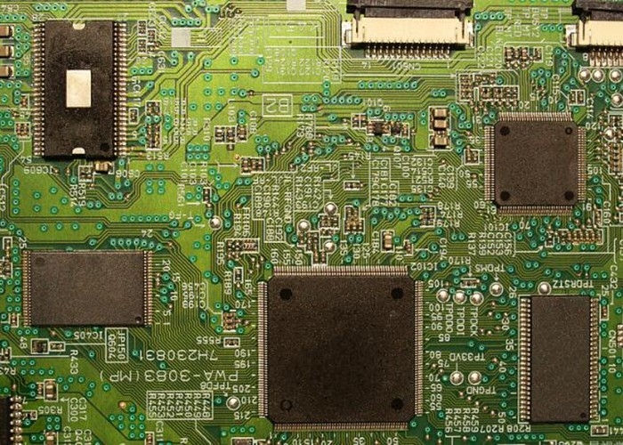
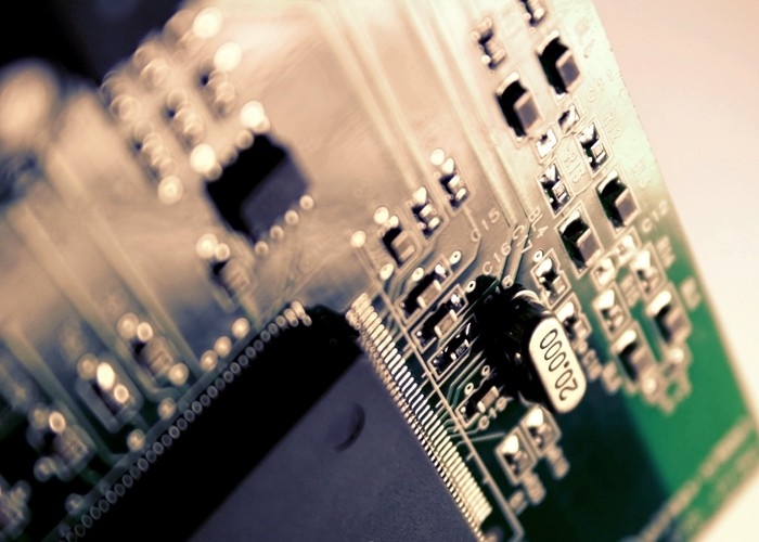
PCBA CAPABILITIES
| Base material | FR4,High-TG FR4,CEM3,aluminum, High frequency(Rogers,Taconic,Aron,PTFE,) |
| Layers | 1-46 |
| Copper Thickness | 0.3oz,0.5oz, 1oz, 2oz, 3oz,4oz,5oz, 6oz |
| Dielectric Thickness | 0.05mm, 0.075mm, 0.1mm,0.15mm,0.2mm |
| board Core Thickness | 0.4mm,0.6mm, 0.8mm, 1.0mm, 1.2mm, |
| 1.5mm, 2.0mm, 3.0mm and 3.2mm | |
| Board Thickness | 0.3mm - 4.0mm |
| Thickness Tolerance | +/-10% |
| Surface Finishing | HASL lead free,ENIG,Plated Gold,Immersion Gold,OSP |
| Solder Mask Color | Green, Blue, Black, White, Yellow, Red, Matt Green, Matt Black, Matt Blue |
| Legend Color | Black, White etc |
| Assembly Types | Surface mount |
| Thro-hole | |
| Mixed technology (SMT & Thru-hole) | |
| Single or double sided placement | |
| Conformal coating | |
| Shield cover assembly for EMI emission control | |
| Parts Procurement | Full Turnkey, Partial Turnkey, Kitted / Consigned |
| Component types | SMT 01005 or larger |
| BGA 0.4mm pitch, POP (Package on Package) | |
| WLCSP 0.35mm pitch | |
| Hard metric connectors | |
| Cable & wire | |
| Other Techniques | Free DFM Review |
| Box Build Assembly | |
| 100% AOI test and X-ray test for BGA | |
| Components cost-down | |
| Function test as custom | |
| Protection technology |
Drilling---Exposure---Plating---Etaching & Stripping---Punching---Electrical Testing---SMT--Wave Soldering---Assembling---ICT--Function Testing---Temperature & Humidity Testing
![]()
![]()
| Product Type | Qty | Normal lead time | Quick-turn lead time |
| SMT+DIP | 1-50 | 1WD-2WD | 8H |
| SMT+DIP | 51-200 | 2WD-3WD | 1.5WD |
| SMT+DIP | 201-2000 | 3WD-4WD | 2WD |
| SMT+DIP | ≥2001 | 4WD-5WD | 3WD |
| PCBA(2-4Layer) | 1-50 | 2.5WD-3.5WD | 1WD |
| PCBA(2-4Layer) | 51-2000 | 5WD-6WD | 2.5WD |
| PCBA(2-4Layer) | ≥2001 | ≥7WD | 5WD |
| PCBA(6-10Layer) | 1-50 | 3WD-4WD | 2.5WD |
| PCBA(6-10Layer) | 51-2000 | 7WD-8WD | 6WD |
| PCBA(10-HDILayer) | 1-50 | 7WD-9WD | 5WD |
| PCBA(10-HDILayer) | 51-2000 | 9WD-11WD | 7WD |
Printed circuit boards And PCB Assembly are mainly used for many communication industry ,Aprospace ,Auto Industry ,Communication,Indutrial Control ,Medical device ,Smart Home,consumer electronics ,automotive electronics , audio and video, optoelectronics, robotics, hydroelectric power, aerospace, education, power supply, printer ,Auto Industry ,Smart Home.etc.
![]()
![]()
Workshop
![]()
![]()
![]()
1.PCB: Vacuum packaging with carton box
2.PCBA: ESD packaging with carton box
![]()
![]()
BEIJING HAINA LEAN TECHNOLOGY CO., LTD offers full serial electronics production services for worldwide customers: everything from the initial idea to the start of mass production based on client's individual needs and technical requirements.
Our services cover all industries and reach all parts of the world.