-
High Light
FR4 HASL Lead Free PCBA
,AOI Lead Free PCBA
,Pb Free AOI PCB Assembly
-
Product NameLead Free PCB Assembly
-
LayersDouble Side ,Multilayer (Custom)
-
Copper Thickness0.3oz-6oz
-
Min. Line Spacing0.030mm/0.030mm
-
Board Thickness0.3-3.5mm
-
Min. Hole SizeLaser 0.05mm ; Mechnical 0.15
-
Surface FinishingHASL,OSP,ENIG,HASL Lead Free,Immersion Gold
-
Solder Mask ColorGreen, Yellow, Red, Black, Blue, Whiteetc
-
Solder TypeWater Soluble Solder Paste, Leaded And Lead-Free
-
TestingFlying Probe Test,X-ray Inspection AOI Test
-
Base MaterialHigh Tg FR-4, Halogen Free FR-4, Thick Copper FR-4, Aluminium Based, Rogers, Taconic
-
ApplicationTelecom Communication ;Military & ; Automotive Industry ;Industrial Control ;Consumer Electronics Office Equipment;Household ;Aerospace; Elevator; High Speed Railway.
-
Place of OriginCHINA
-
Brand NameHNL-PCBA
-
CertificationISO9001,IS16949, ISO14001,ROHS ,IPC-A ,QC080000
-
Model NumberPCB Assembly
-
Minimum Order Quantity1 PC
-
PriceNegotiable
-
Packaging DetailsESD packaging with carton box
-
Delivery Time1-7days
-
Payment TermsT/T, Western Union, L/C, MoneyGram
-
Supply Ability10,000,000 Point /Day
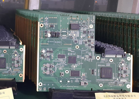
AOI Test X RAY FR4 HASL Lead Free PCBA

AOI Test X-RAY One Stop FR4 HASL Lead Free PCB Assembly
PCB Assembly Introduction
Our assembly process has been designed to meet all variations of PCBs, including single- or double-sided boards, Multilayer , rigid ,flexible circuits and Mixed technology. We run both leaded and RoHS/Lead-Free Surface Mount Technology (SMT) lines as well as wave solder equipment for both RoHS and leaded processes. Our manufacturing process allows for the highest quality product through process automation, environmental controls, automatic optical inspection (AOI) and flying probe at the best competitive price.
PCB CAPABILITIES
| FACTORY CAPABILITIES | |||
| No. | Items | 2019 | 2020 |
| 1 | HDI Capabilities | HDI ELIC (4+2+4) | HDI ELIC(5+2+5) |
| 2 | Max layer count | 32L | 36L |
| 3 | Board Thickness | Core thickness 0.05mm-1.5mm ,Fineshed board thickness 0.3-3.5mm | Core thickness 0.05mm-1.5mm ,Fineshed board thickness 0.3-3.5mm |
| 4 | Min.Hole Size |
Laser 0.075mm Mechnical 0.15 |
Laser 0.05mm Mechnical 0.15 |
| 5 | Min Line Width/Space | 0.035mm/0.035 | 0.030mm/0.030mm |
| 6 | Copper Thickness | 1/3oz-4oz | 1/3oz-6oz |
| 7 | Size Max Panel size | 700x610mm | 700x610mm |
| 8 | Registration Accuracy | +/-0.05mm | +/-0.05mm |
| 9 | Routing Accuracy | +/-0.075mm | +/-0.05mm |
| 10 | Min.BGA PAD | 0.15mm | 0.125mm |
| 11 | Max Aspect Ratio | 10:1 | 10:1 |
| 12 | Bow and Twist | 0.50% | 0.50% |
| 13 | Impedance Control Tolerance | +/-8% | +/-5% |
| 14 | Daily output | 3,000m2 (Max capacity of equipment) | 4,000m2 (Max capacity of equipment) |
| 15 | Surface Finishing | HASL Lead Free /ENEPING /ENIG /HASL /FINGER GOLD/IMMERSION TIN/SELECTIVE THICK GOLD | |
| 16 | Raw Material | FR-4/Normal Tg/High Tg/Low Dk/HF FR4/PTEE/PI | |
PCBA CAPABILITIES
| PCBA Capability | |||
| Material Type | Item | Min | Max |
| PCB | Dimension (length,width,height.mm) | 50*40*0.38 | 600*400*4.2 |
| Material | FR-4,CEM-1,CEM-3,Aluminium-based board,Rogers,ceramic plate,FPC | ||
| Surface finish | HASL,OSP,Immersion gold,Flash Gold Finger | ||
| Components | Chip&IC | 1005 | 55mm |
| BGA Pitch | 0.3mm | - | |
| QFP Pitch | 0.3mm | - | |
Lead free PCB Assembly Production Process
PCB,Component sourcing ,QC ,SMT Process ,AOI ,Test ,Automatic optical inspection ,DIP Process ,Washing board ,FQC .
![]()
WorkShop
![]()
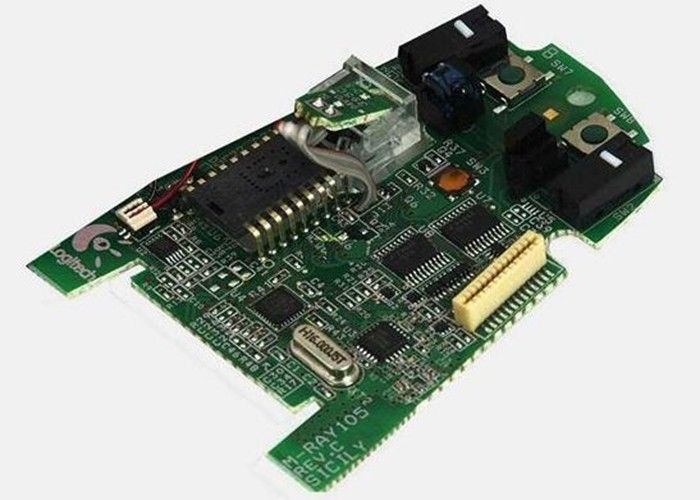
Products Show
![]()
Application Field
Printed circuit boards And PCB Assembly are mainly used for many communication industry, medical equipments, consumer electronics and automobile industry ,automotive electronics , audio and video, optoelectronics, robotics, hydroelectric power, aerospace, education, power supply, printer etc industries.
![]()
Delivery Time
| Product Type | Qty | Normal lead time | Quick-turn lead time |
| SMT+DIP | 1-50 | 1WD-2WD | 8H |
| SMT+DIP | 51-200 | 2WD-3WD | 1.5WD |
| SMT+DIP | 201-2000 | 3WD-4WD | 2WD |
| SMT+DIP | ≥2001 | 4WD-5WD | 3WD |
| PCBA(2-4Layer) | 1-50 | 2.5WD-3.5WD | 1WD |
| PCBA(2-4Layer) | 51-2000 | 5WD-6WD | 2.5WD |
| PCBA(2-4Layer) | ≥2001 | ≥7WD | 5WD |
| PCBA(6-10Layer) | 1-50 | 3WD-4WD | 2.5WD |
| PCBA(6-10Layer) | 51-2000 | 7WD-8WD | 6WD |
| PCBA(10-HDILayer) | 1-50 | 7WD-9WD | 5WD |
| PCBA(10-HDILayer) | 51-2000 | 9WD-11WD | 7WD |
Partners
![]()
Common packaging
PCB: Vacuum packaging with carton box
PCBA: ESD packaging with carton box
![]()
Certification
![]()
FAQ
Q1:What kind of PCB file format can you accept for production?
Gerber, PROTEL 99SE, PROTEL DXP, CAM350, ODB+(.TGZ)
Q2:Is my PCB files safe when I submit them to you for manufacturing?
We respect customer's copyright and will never manufacture PCB for someone else with your files unless we receive written permission from you, nor we'll share these files with any other 3rd parties.
Q3:What payments do you accept ?
-Telex Transfer(T/T),Western Union,Letter of Credit(L/C)
-Paypal,AliPay,Credit Card
Q4:How to get the PCB?
A:For small packages, we will ship the boards to you by DHL,UPS,FedEx,EMS. Door to door service! You will get your PCBs at your home.
B:For heavy goods more than 300kg, we may ship your boards by ship or by air to save freight cost. Of course, if you have your own forwarder, we may contact them for dealing with your shipment.
Q5:What is your minimum order quantity?
Our MOQ is 1 PCS.
Q6: Can we visit your company?
No problem. You are welcome to visit us in Beijing. Or the branch factory is in Tianjin.
Q7: How can you ensure the quality of the PCB?
Our PCBs are 100% test including Flying Probe Test, E-test and AOI.
Company Information
Beijing Haina lean Electronics Co.,Ltd is one of the most professional PCB manufacture in Beijing,China. With more then 10 years of development, Haina Lean Electronics turns into a first class manufacture of HDI PCB ,with production capability 4000 square meters.
Our factory is providing high quality bare PCB, PCB layout design service and PCB assembly service,including components sourcing, function test,conformal coating and complete assembly for clients all.
We have profuse experience in manufacturing PCB,owned experienced technical R & D technology team, young and professional sales and customer service team, experienced and professional procurement team and assembly testing team, which make sure the products quality of the pass rate, on-time delivery rate of customer orders.
Our services include: circuit board design and layout, 2-46 layers PCB manufacturing, professional FPC production, electronic components purchasing, SMT professional processing, Soldering and Assembly, especially sample and small bulk orders. we have the advantages of a quick quote, fast production, fast delivery.
The company pursues "inclusiveness, excellence, people-oriented". Constantly innovate, take technology as the core, regard quality as life, and wholeheartedly provide customers with high-quality and high-efficiency humanized services.We are willing to serve our customers with the principle of continuous honesty & trustworthiness, pragmatism and innovation.
![]()
Our services cover all industries and reach all parts of the world.