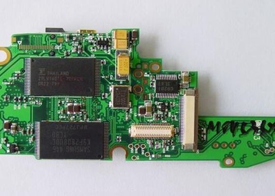
BGA X Ray Inspection Lead Free PCB Assembly For Telecom Communication
-
High Light
1.2mm Lead Free PCB Assembly
,BGA Lead Free PCB Assembly
,ISO9001 BGA PCB Assembly
-
Product NameGreen Red Yellow Blue PCBA
-
Layers1-46layers Custom
-
Copper Thickness0.3oz 1oz 2oz 3oz ..... 6oz
-
Min. Line Spacing0.030mm/0.030mm
-
Board Thickness0.3 , 0.5 , 1.2 , 1.6 ,,,,,,, 3.5mm
-
Min. Hole SizeLaser 0.05mm ; Mechnical 0.15
-
Solder Mask ColorGreen, Yellow, Red, Black, Blue, Whiteetc
-
MaterialFR-4/Normal Tg/High Tg/Low Dk/HF FR4/ Aluminium
-
Surface FinishingHASL,OSP,ENIG,HASL Lead Free,Immersion Gold
-
ApplicationTelecom Communication ; Automotive Industry ;Industrial Control ;Consumer Electronics Office Equipment;Household ;Aerospace; Elevator; High Speed Railway.
-
Place of OriginCHINA
-
Brand NameHNL-PCBA
-
CertificationISO9001,IS16949, ISO14001,ROHS ,IPC-A ,QC080000
-
Model NumberPCB Assembly
-
Minimum Order Quantity1 PC
-
PriceNegotiable
-
Packaging DetailsESD packaging with carton box
-
Delivery Time1-7days
-
Payment TermsT/T, Western Union, L/C, MoneyGram
-
Supply Ability10,000,000 Point /Day
BGA X Ray Inspection Lead Free PCB Assembly For Telecom Communication
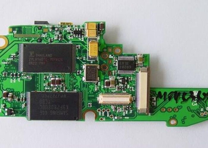
HASL Lead Free PCB BGA X Ray Inspection Green Red Yellow Blue PCBA
PCB Assembly Introduction
The list of these electronic components include-Resistor;SMD capacitor;Transformer;Diode;ICs;Transmitter;etc.
The PCBA electronic components have two types.
1. SMD components
2. Through-hole components
PCBA refers to the complete electronic circuit board after all components have been assembled . It has many benefits that make it a much sought-after element in the communicating and electronics industry.
The PCBA is a complete assembly. You have to assemble the PCB, once it is ready. The assembling requires both passive and active components.
Factory Capabilities
| PCB Assembly Capability | ||
| Item | Capability | |
| Advantages | Professional Surface-mounting and Through-hole soldering technology | |
| Various sizes like 1206,0805,0603 components SMT technology | ||
| ICT(In Circuit Test),FCT(Functional Circuit Test) | ||
| PCB Assembly With UL,ISODD,Rohs Approval | ||
| SMT process adpot reflow soldering technology | ||
| High Standard SMT & Solder Assembly Line | ||
| HDI technology (High density interconnected board placement technology capacity) | ||
| Components | Chip & IC 01005 ,55mm | |
| BGA pitch 0.3mm | ||
| QFP Pitch 0.3mm | ||
| Quantity | Prototype & Low Volume PCB Assembly,from 1 Board to 250, or up to 5000 and customized | |
| Type of Assembly | SMT, Thru-hole ,DIP ,MIX | |
| Solder Type | Water Soluble Solder Paste, Leaded and Lead-Free | |
| Bare Board Size | Largest:700X610mm (Custom) | |
| File Formate | Gerber files, Pick-N-Place file, BOM ,PADs ,Protel,CAD | |
| Types of Service | Turn-key,partial turn-key or consignment | |
| Testing | Flying Probe Test,X-ray Inspection AOI Test | |
| PCB assembly process | Drilling----Exposure-----Plating-----Etaching & Stripping---Punching-----Electrical Testing-----SMT-----Wave Soldering-----Assembling---- ICT-----Function Testing-----Temperature & Humidity Testing | |
Lead free PCB Aassembly Production Process
PCB,Component sourcing ,QC ,SMT Process ,AOI ,Test ,Automatic optical inspection ,DIP Process ,Washing board ,FQC .
![]()
Our WorkShop
![]()
![]()
![]()
![]()
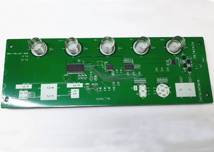
Green Red Yellow Blue PCBA Application Field
Printed circuit boards And PCB Assembly are mainly used for many telecom communication industry, medical equipments, consumer electronics ,automotive electronics , audio and video, optoelectronics, robotics, hydroelectric power, aerospace, education, power supply, printer ,Auto Industry ,Smart Home.etc.
Delivery Time
| Product Type | Qty | Normal lead time | Quick-turn lead time |
| SMT+DIP | 1-50 | 1WD-2WD | 8H |
| SMT+DIP | 51-200 | 2WD-3WD | 1.5WD |
| SMT+DIP | 201-2000 | 3WD-4WD | 2WD |
| SMT+DIP | ≥2001 | 4WD-5WD | 3WD |
| PCBA(2-4Layer) | 1-50 | 2.5WD-3.5WD | 1WD |
| PCBA(2-4Layer) | 51-2000 | 5WD-6WD | 2.5WD |
| PCBA(2-4Layer) | ≥2001 | ≥7WD | 5WD |
| PCBA(6-10Layer) | 1-50 | 3WD-4WD | 2.5WD |
| PCBA(6-10Layer) | 51-2000 | 7WD-8WD | 6WD |
| PCBA(10-HDILayer) | 1-50 | 7WD-9WD | 5WD |
| PCBA(10-HDILayer) | 51-2000 | 9WD-11WD | 7WD |
Partners
![]()
Common packaging
PCB: Vacuum packaging with carton box
PCBA: ESD packaging with carton box
![]()
FAQ
Q1:What service do you have?
A1: We provide turnkey solution including RD, PCB fabrication, SMT, PCB Assembley ,final assembly,testing and other
value-added service.
Q2:What are the main products of your PCB/PCBA services?
A2:Our PCB/PCBA services are mainly for the industries including Medical, Automotive, Energy,
Metering/Measurements. Consumer Electronics.
Q3:How can we ensure our information should not let third party to see our design?
A3: We are wiling to sign NDA effect by customer side locallaw and promising to keep customers datain highconfidential level.
Q4:What does Parason need for a customized PCB order?
A4:When you place a PCB order, the customers need to provide Gerber or pcb file.If you do not have the fileinthe correct format, you can send all the details related to the products.
Q5:What will be needed for a customized PCBA order?
A5: When you place a PCBA order, you need to provide Gerber or pcb file and the BOM list to us.
Q6:Do you have an minimum order quantity?
A6:We accept order with as low as a quantity of 1 (piece or panel)
Our services cover all industries and reach all parts of the world.