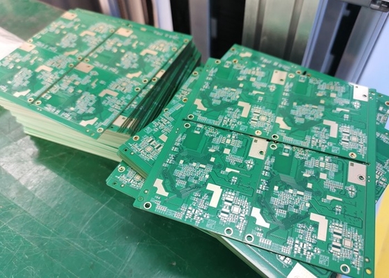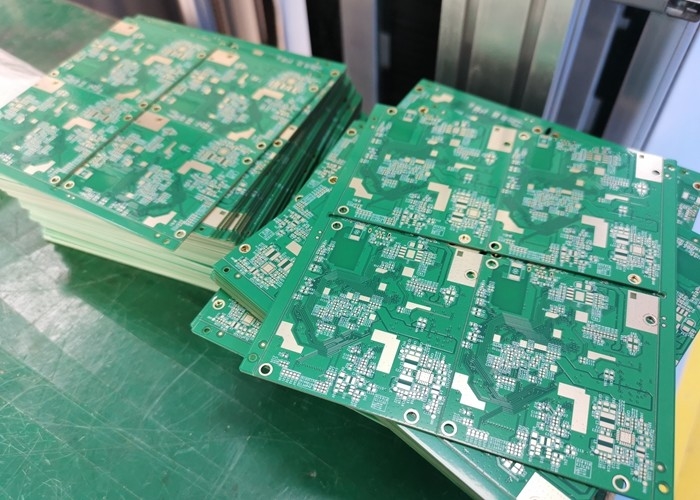
Beijing HaiNa Lean focuses on PCB manufacturing and PCB assembly. We have strong technology engineering team , a professional procurement team and testing team to ensure the quality. We provide one-stop service, including PCB manufacturing,electronic components sourcing, and PCB assembly as well as testing.
| FACTORY CAPABILITIES | |||
| No. | Items | 2019 | 2020 |
| 1 | HDI Capabilities | HDI ELIC (4+2+4) | HDI ELIC(5+2+5) |
| 2 | Max layer count | 32L | 36L |
| 3 | Board Thickness | Core thickness 0.05mm-1.5mm ,Fineshed board thickness 0.3-3.5mm | Core thickness 0.05mm-1.5mm ,Fineshed board thickness 0.3-3.5mm |
| 4 | Min.Hole Size | Laser 0.075mm | Laser 0.05mm |
| Mechnical 0.15mm | Mechnical 0.15mm | ||
| 5 | Min Line Width/Space | 0.035mm/0.035mm | 0.030mm/0.030mm |
| 6 | Copper Thickness | 1/3oz-4oz | 1/3oz-6oz |
| 7 | Size Max Panel size | 700x610mm | 700x610mm |
| 8 | Registration Accuracy | +/-0.05mm | +/-0.05mm |
| 9 | Routing Accuracy | +/-0.075mm | +/-0.05mm |
| 10 | Min.BGA PAD | 0.15mm | 0.125mm |
| 11 | Max Aspect Ratio | 10:1 | 10:1 |
| 12 | Bow and Twist | 0.50% | 0.50% |
| 13 | Impedance Control Tolerance | +/-8% | +/-5% |
| 14 | Daily Output | 3,000m2 (Max capacity of equipment) | 4,000m2 (Max capacity of equipment) |
| 15 | Surface Finishing | ENEPING /ENIG /HASL /FINGER GOLD/IMMERSION TIN/SELECTIVE THICK GOLD | |
| 16 | Raw Material | FR-4/Normal Tg/High Tg/Low Dk/HF FR4/PTEE/PI | |
Immersion gold ,Lead-free HASL,OSP,etc.
![]()
![]()
Our service
| Electronic Manufacturing Service | PCB Electronic Design |
| PCB Electronic Design | PCB Layout Service |
| PCB Assembly process service | PCBA Components Sourcing |
![]()
| Prototype PCB | Batch | Prototype | Expedited |
| Double sides | 9 Days | 5 Days | 45h |
| Four-layer | 10 Days | 5 Days | 3 Days |
| Six-layer | 12 Days | 6 Days | 3 Days |
| Eight-layer | 12 Days | 7 Days | 4 Days |
| Ten-layer | 14 Days | 10 Days | 4Days |
| Twelve-layer | 14 Days | 10 Days | 5 Days |
| Fourteen-layer | 16 Days | 12Days | 6 Days |
| Sixteen-layer | 16 Days | 12 Days | 6 Days |
| Eighteen-layer | 18 Days | 14 Days | 6 Days |
| Twenty-layer | 18 Days | 14 Days | 10 Days |
| Twenty two-layer | 20 Days | 14 Days | 10 Days |
| Twenty four-layer | 20 Days | 14 Days | 10 Days |
| Twenty six-layer | 20 Days | 14 Days | 10 Days |
| Twenty eight-layer | 20 Days | 14 Days | 10 Days |
FR4 Printed Circuit Board Application Field
Printed circuit boards And PCB Assembly are mainly used for many communication industry, medical equipments, consumer electronics ,automotive electronics , audio and video, optoelectronics, robotics, hydroelectric power, aerospace, education, power supply, printer ,Auto Industry ,Smart Home.etc.
![]()
![]()
![]()
![]()
![]()
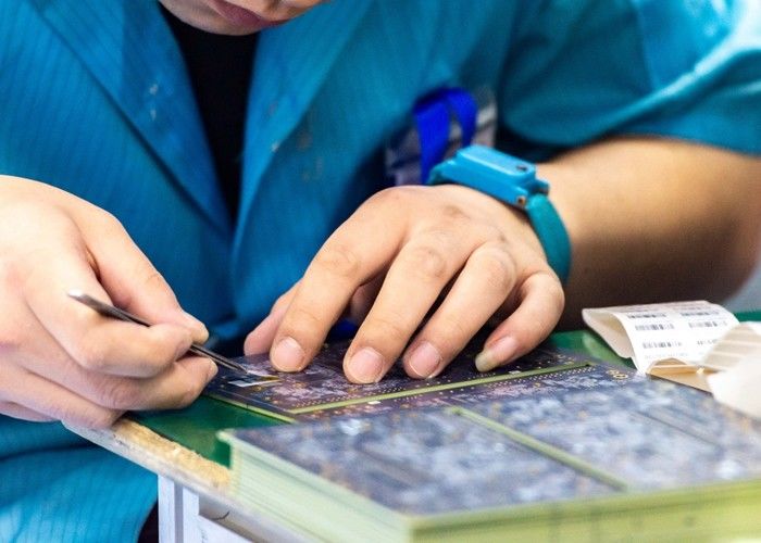
Testing service
1. Manual visual inspection of PCB board
2. PCB board online test
3. PCB board function test
4. AOI (Automatic optical inspection)
5. Automatic X-ray inspection
6. Laser detection system
7. Size detection
Above is the PCB testing service.
Haina lean Electronics provides custom test service according to client's requirements and products.
Usually Haina lean Electronics Co.,Ltd PCBA Tech offers a full range of testing service. Including:
1. AOI(Automatic Optical Inspection)
2. Function Testing
3. In Circuit Testing
4. Testing Jig
5. Testing Service
6. X-Ray for BGA Testing
7. Printing Solder Paste Test
Each board is carefully examined by our dedicated inspection team using AOI and high magnification viewers.
Using our X-Ray machine, we test PCBs to component level and all wiring is fully inspected and tested.
Flash testing and earth bonding tests can also be undertaken where required.
![]()
Partners
![]()
PCB: Vacuum packaging with carton box
PCBA: ESD packaging with carton box
![]()
Why choose us?
Welcome to visit our factory, Haina lean Electronics Co., Ltd.
1. Experienced: Focus on PCB And PCBA munufacturing over 10 years.
2. Professional: Expertise engineer with barrier-free English
3. Rapid delivery: On-time delivery rate reaches 98%
4.Cost effective: No excessive profits. Lower cost with same quality And service
Company Information
Beijing Haina lean Electronics Co.,Ltd is one of the most professional PCB manufacture in Beijing,China. With more then 10 years of development, Haina Lean Electronics turns into a first class manufacture of HDI PCB ,with production capability 4000 square meters.
Our factory is providing high quality bare PCB, PCB layout design service and PCB assembly service,including components sourcing, function test,conformal coating and complete assembly for clients all.
We have profuse experience in manufacturing PCB,owned experienced technical R & D technology team, young and professional sales and customer service team, experienced and professional procurement team and assembly testing team, which make sure the products quality of the pass rate, on-time delivery rate of customer orders.
Our services include: circuit board design and layout, 2-46 layers PCB manufacturing, professional FPC production, electronic components purchasing, SMT professional processing, Soldering and Assembly, especially sample and small bulk orders. we have the advantages of a quick quote, fast production, fast delivery.
![]()
Our services cover all industries and reach all parts of the world.