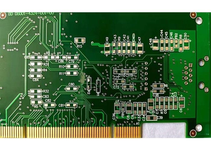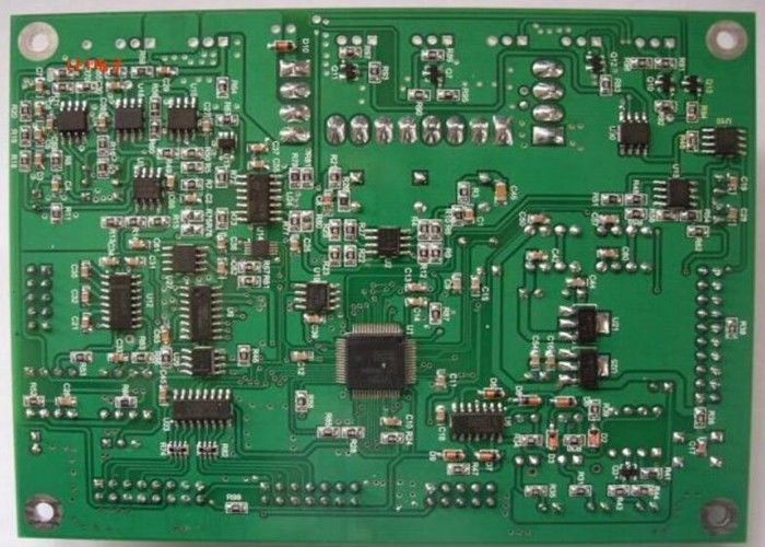
The double-sided printed circuit board (also double-layer board)provides on both side conductive paths for assembly of components, then to fabricate the PCB'A.
Single sided printed circuit board assembly; double sided printed circuit board assembly
single layer PCBA ; double layer PCBA; multilayer PCBA.
Haina lean Electronics is a one-stop EMS supplier integrating PCB design, PCB manufacturing, Component sourcing and PCB assembly.
The company is specialized in electronic products supporting processing services, mainly to undertake circuit board design, layout production, components procurement, PCB plate making, circuit board welding assembly debugging and other OEM/ODM services.
| No. | Items | |
| 1 | HDI Capabilities | HDI ELIC(5+2+5) |
| 2 | Max layer count | 36L |
| 3 | Board Thickness | Core thickness 0.05mm-1.5mm ,Fineshed board thickness0.3-3.5mm |
| 4 | Min.Hole Size |
Laser 0.05mm Mechnical 0.15 |
| 5 | Min Line Width/Space | 0.030mm/0.030mm |
| 6 | Copper Thickness | 1/3oz-6oz |
| 7 | Size Max Panel size | 700x610mm |
| 8 | Registration Accuracy | +/-0.05mm |
| 9 | Routing Accuracy | +/-0.05mm |
| 10 | Min.BGA PAD | 0.125mm |
| 11 | Max Aspect Ratio | 10:1 |
| 12 | Bow and Twist | 0.50% |
| 13 | Impedance Control Tolerance | +/-5% |
| 14 | Daily output | 4,000m2 (Max capacity of equipment) |
| 15 | Surface Finishing | ENEPING /ENIG /HASL /FINGER GOLD/IMMERSION TIN/SELECTIVE THICK GOLD |
| 16 | Raw Material | FR-4/Normal Tg/High Tg/Low Dk/HF FR4/PTEE/PI |
| PCBA Capability | ||||||
| Material type | PCB | Components | ||||
| Item | Dimension (Length, width,height. mm) | Material | Surface finish | Chip&IC | BGA Pitch | QFP Pitch |
| Min | 50*40*0.38 | FR-4,CEM-1,CEM-3,Aluminium-based board,Rogers,ceramic plate,FPC | HASL, OSP, Immersion gold, Flash Gold Finger | 1005 | 0.3mm | 0.3mm |
| Max | 600*400*4.2 | |||||
PCB Fabrication Assembly Process
1.Solder Paste stenciling---2.Surface Mount Technology (Pick and Place)---3.Reflow Soldering---4.Inspection and Quality Control---5.Through-Hole Component Insertion (DIP Process)---6.Final Inspection and Functional Test
![]()
1.Service value
Independent quotation system to quickly serve the market
2.PCB manufacturing
High-tech PCB and PCB assembly production line
3.Material purchasing
A team of experienced electronic component procurement engineers
4.SMT post soldering
Dust-free workshop, high-end SMT patch processing
![]()
1. We are the manufacturer/ factory; Welcome to visit us one day.
2. We have good quality control systems, including AOI, ISO 9001 etc. ;
3. All the material we use have the RoHS identify;
4. All the components we use are the New & Original;
5. One-stop service can be provided from PCB design, 1-36 layers PCB manufacturing, components sourcing, PCB Assembly, to Fully Product Assembly.
![]()
Printed circuit boards And PCB Assembly are mainly used for many communication industry, medical equipments, consumer electronics and automobile industry ,automotive electronics , audio and video, optoelectronics, robotics, hydroelectric power, aerospace, education, power supply, printer etc industries.
![]()
Workshop
![]()
![]()
1.PCB: Vacuum packaging with carton box
2.PCBA: ESD packaging with carton box
![]()
![]()
Our services cover all industries and reach all parts of the world.