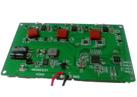

Using state-of-the-art Surface Mount and Through-Hole Technology, we can provide simple one-sided to complex double-sided electronic circuit boards. Haina Lean Technology CO., LTD is a professional factory. We build amazing electronics. From prototype to production, we are entrusted to be their electronic manufacturing partner by companies small and large around the world.
PCBA CAPABILITIES
| Base material | FR4,High-TG FR4,CEM3,aluminum, High frequency(Rogers,Taconic,Aron,PTFE,) |
| Layers | 1-46 |
| Copper Thickness | 0.3oz,0.5oz, 1oz, 2oz, 3oz,4oz,5oz, 6oz |
| Dielectric Thickness | 0.05mm, 0.075mm, 0.1mm,0.15mm,0.2mm |
| board Core Thickness | 0.4mm,0.6mm, 0.8mm, 1.0mm, 1.2mm, |
| 1.5mm, 2.0mm, 3.0mm and 3.2mm | |
| Board Thickness | 0.3mm - 4.0mm |
| Thickness Tolerance | +/-10% |
| Surface Finishing | HASL lead free,ENIG,Plated Gold,Immersion Gold,OSP |
| Solder Mask Color | Green, Blue, Black, White, Yellow, Red, Matt Green, Matt Black, Matt Blue |
| Legend Color | Black, White etc |
| Assembly Types | Surface mount |
| Thro-hole | |
| Mixed technology (SMT & Thru-hole) | |
| Single or double sided placement | |
| Conformal coating | |
| Shield cover assembly for EMI emission control | |
| Parts Procurement | Full Turnkey, Partial Turnkey, Kitted / Consigned |
| Component types | SMT 01005 or larger |
| BGA 0.4mm pitch, POP (Package on Package) | |
| WLCSP 0.35mm pitch | |
| Hard metric connectors | |
| Cable & wire | |
| Other Techniques | Free DFM Review |
| Box Build Assembly | |
| 100% AOI test and X-ray test for BGA | |
| Components cost-down | |
| Function test as custom | |
| Protection technology |
PCB assembly process
PCB: Drilling--Exposure--Plating--Etaching & Stripping--Punching--Electrical Testing--SMT--Wave Soldering--Assembling--ICT--Function Testing--Temperature & Humidity Testing
PCBA : 1.Solder Paste stenciling---2.Surface Mount Technology (Pick and Place)---3.Reflow Soldering---4.Inspection and Quality Control---5.Through-Hole Component Insertion (DIP Process)---6.Final Inspection and Functional Test
![]()
1.Service value
Independent quotation system to quickly serve the market
2.PCB manufacturing
High-tech PCB and PCB assembly production line
3.Material purchasing
A team of experienced electronic component procurement engineers
4.SMT post soldering
Dust-free workshop, high-end SMT patch processing
![]()
| Product Type | Qty | Normal lead time | Quick-turn lead time |
| SMT+DIP | 1-50 | 1WD-2WD | 8H |
| SMT+DIP | 51-200 | 2WD-3WD | 1.5WD |
| SMT+DIP | 201-2000 | 3WD-4WD | 2WD |
| SMT+DIP | ≥2001 | 4WD-5WD | 3WD |
| PCBA(2-4Layer) | 1-50 | 2.5WD-3.5WD | 1WD |
| PCBA(2-4Layer) | 51-2000 | 5WD-6WD | 2.5WD |
| PCBA(2-4Layer) | ≥2001 | ≥7WD | 5WD |
| PCBA(6-10Layer) | 1-50 | 3WD-4WD | 2.5WD |
| PCBA(6-10Layer) | 51-2000 | 7WD-8WD | 6WD |
| PCBA(10-HDILayer) | 1-50 | 7WD-9WD | 5WD |
| PCBA(10-HDILayer) | 51-2000 | 9WD-11WD | 7WD |
Our products are widely used in communication equipment, industrial control, consumer electronics, medical equipment, aerospace, light-emitting diode lighting, automotive electronics etc.
![]()
Workshop
![]()
![]()
1.PCB: Vacuum packaging with carton box
2.PCBA: ESD packaging with carton box
![]()
![]()
Haina lean Electronics Co., Ltd is a one-stop EMS supplier integrating PCB design, PCB manufacturing, Component sourcing and PCB assembly.
Here is strong component supply chain and procceurement team. Prototype and mass production are available. Competitive price is for high-quality and services. Exported to worldwide customer in US, Europe, Canada.