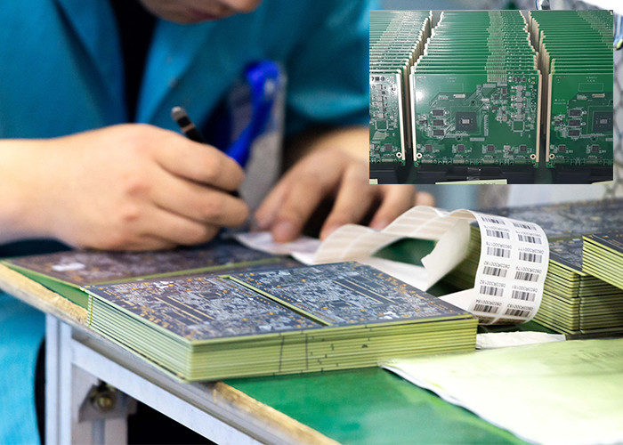
Printed circuit board assembly is the process of connecting the wiring of the printed circuit board with the electronic components. Traces or conductive paths engraved on the PCB laminate copper board are used in non-conductive substrates to form components.
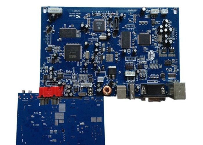
Haina Lean PCBA capabilities: SMT assembly, BGA assembly, through-hole assembly, mixed assembly, high-density connection PCB (HDI PCB) , rigid Flex PCB assembly services.
About our One-stop PCB manufacturing and assembly:
1. Component procurement: We have many years of experience and stable relationships with authorized electronic component manufacturers and distributors, so you can always get genuine high-quality parts. All parts undergo 100% quality inspection before use.
2. Comprehensive quality assurance: From visual inspection to AOI and X-ray inspection, we attach great importance to quality control and strictly test all functions and quality.
3. Professional engineering team: The development of Haina lean Electronics is inseparable from the performance and engagement of PCBA employees.The skills, professional knowledge and talent advantage of each PCBA employee are the core of Haina lean Electronics.
4. Mass PCB assembly: We are as proficient in handling large PCB assembly orders as delivering small orders.
5. Fully turnkey PCB assembly: our turnkey PCB assembly allows us to take care of your entire project from start to finish, so you can step in and start taking advantage of the finished product right away.
6. Certification: Passed ISO 9001:2008 certification and complies with RoHS standards, including IPC 610 Class 2 and Class 3.
| FACTORY CAPABILITIES | |||
| No. | Items | 2019 | 2020 |
| 1 | HDI Capabilities | HDI ELIC (4+2+4) | HDI ELIC(5+2+5) |
| 2 | Max layer count | 32L | 36L |
| 3 | Board Thickness | Core thickness 0.05mm-1.5mm ,Fineshed board thickness 0.3-3.5mm | Core thickness 0.05mm-1.5mm ,Fineshed board thickness 0.3-3.5mm |
| 4 | Min.Hole Size |
Laser 0.075mm Mechnical 0.15 |
Laser 0.05mm Mechnical 0.15 |
| 5 | Min Line Width/Space | 0.035mm/0.035 | 0.030mm/0.030mm |
| 6 | Copper Thickness | 1/3oz-4oz | 1/3oz-6oz |
| 7 | Size Max Panel size | 700x610mm | 700x610mm |
| 8 | Registration Accuracy | +/-0.05mm | +/-0.05mm |
| 9 | Routing Accuracy | +/-0.075mm | +/-0.05mm |
| 10 | Min.BGA PAD | 0.15mm | 0.125mm |
| 11 | Max Aspect Ratio | 10:1 | 10:1 |
| 12 | Bow and Twist | 0.50% | 0.50% |
| 13 | Impedance Control Tolerance | +/-8% | +/-5% |
| 14 | Daily output | 3,000m2 (Max capacity of equipment) | 4,000m2 (Max capacity of equipment) |
| 15 | Surface Finishing | HASL Lead Free /ENEPING /ENIG /HASL /FINGER GOLD/IMMERSION TIN/SELECTIVE THICK GOLD | |
| 16 | Raw Material | FR-4/Normal Tg/High Tg/Low Dk/HF FR4/PTEE/PI | |
| PCBA Capability | |||
| Material Type | Item | Min | Max |
| PCB | Dimension (length,width,height.mm) | 50*40*0.38 | 600*400*4.2 |
| Material | FR-4,CEM-1,CEM-3,Aluminium-based board,Rogers,ceramic plate,FPC | ||
| Surface finish | HASL,OSP,Immersion gold,Flash Gold Finger | ||
| Components | Chip&IC | 1005 | 55mm |
| BGA Pitch | 0.3mm | - | |
| QFP Pitch | 0.3mm | - | |
![]()
![]()
| Product Type | Qty | Normal lead time | Quick-turn lead time |
| SMT+DIP | 1-50 | 1WD-2WD | 8H |
| SMT+DIP | 51-200 | 2WD-3WD | 1.5WD |
| SMT+DIP | 201-2000 | 3WD-4WD | 2WD |
| SMT+DIP | ≥2001 | 4WD-5WD | 3WD |
| PCBA(2-4Layer) | 1-50 | 2.5WD-3.5WD | 1WD |
| PCBA(2-4Layer) | 51-2000 | 5WD-6WD | 2.5WD |
| PCBA(2-4Layer) | ≥2001 | ≥7WD | 5WD |
| PCBA(6-10Layer) | 1-50 | 3WD-4WD | 2.5WD |
| PCBA(6-10Layer) | 51-2000 | 7WD-8WD | 6WD |
| PCBA(10-HDILayer) | 1-50 | 7WD-9WD | 5WD |
| PCBA(10-HDILayer) | 51-2000 | 9WD-11WD | 7WD |
Printed circuit boards And PCB Assembly are mainly used for many communication industry, medical equipments, consumer electronics and automobile industry ,automotive electronics , audio and video, optoelectronics, robotics, hydroelectric power, aerospace, education, power supply, printer etc industries.
![]()
![]()
![]()
![]()
PCB: Vacuum packaging with carton box
PCBA: ESD packaging with carton box
![]()
1.What are needed for quotation?
PCB: Quantity, Gerber file and Technic requirements(material,surface finish treatment, copper thickness,board thickness ......)
PCBA: PCB information, BOM, (Testing documents...)
2. What file formats do you accept for production?
Gerber file: CAM350 RS274X
PCB file: Protel 99SE, P-CAD 2001 PCB
BOM: Excel (PDF,word,txt)
3.Are my files safe?
Your files are held in complete safety and security.We protect the intellectual property for our customers in the whole process.. All documents from customers are never shared with any third party.
4.MOQ?
There is no MOQ .We can flexibly handle small and mass production.
5.Shipping Cost ?
The shipping cost is determined by the destination ,weight ,packing size of the goods .We can provide shipping, air, land, express and other transportation services .
6.How to ensure high-quality production?
The process is strictly controlled under ISO 9001:2015 standards.
Most of our advanced equipment and tools are imported from abroad. Such as Flying Probe, X-ray Inspection, AOI (Automated Optical Inspector) and ICT (in-circuit testing).
We have a very professional QC team.
Q7.What are the services you can provide ?
One-stop contract manufacturing
A:PCB Assembly;
B:PCB Design & Layout
C:PCBA programming & functional testing;
D:Electronic components purchasing service;
E:Enclosure molding & final assembly with labels,instructions,enclosure, boxes.
Q8.Whether all PCBA s will be tested before delivery ?
Yes , we will test each piece of PCBA product under your testing methods ,to ensure quality and functionality .
Q9.Do you provide OEM service ?
Yes ,we offer PCB and PCBA OEM Service , we manufacture the PCB and PCBA products to your design and requirements .
Haina lean Electronics Co., Ltd is a one-stop EMS supplier integrating PCB design, PCB manufacturing, Component sourcing and PCB assembly.
Our company was established in May 1, 2012 in Beijing. And expansion was completed in June 2016. The company is specialized in electronic products supporting processing services, mainly to undertake circuit board design, layout production, components procurement, PCB plate making, circuit board welding assembly debugging and other OEM/ODM services.
Our first factory is located in Changping District, Beijing, the main radiation Haidian, Changping, Chaoyang three areas of Beijing. Since our company’s establishment, we have been adhering to creating high quality, high efficiency, low-cost business philosophy based on the circuit board processing industry for customers. Most of the key staff of the company are mature technical talents who have been engaged in the industry for more than 10 years, and have rich experience in the production of SMT and DIP, also has rich experience in production for high density & difficulty to package components such as BGA. The factory covers an area of 1500 square meters. Since its establishment, we obtain a good reputation in the industry through the continuous efforts of all staff and high quality service . Our second branch plant is located in Langfang city, and mainly cover Fengtai and Daxing Yizhuang area.
The company pursues "inclusiveness, excellence, people-oriented". Constantly innovate, take technology as the core, regard quality as life, and wholeheartedly provide customers with high-quality and high-efficiency humanized services.We are willing to serve our customers with the principle of continuous honesty & trustworthiness, pragmatism and innovation.
![]()
Our services cover all industries and reach all parts of the world.