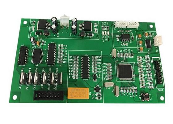
Surface mount technology(SMT) is an area of electronic PCB assembly. SMT PCB fabricating & assembly does not only includes placing and soldering of components but also a wide array productions. We fabricate PCB Assembly with SMT,DIP, BGA, QFP, as well as THT selective soldering. Our engineers is qualified and experienced in producing surface-mount (SMT), through-hole (THT) and mixed-technology components and fine-pitch parts and ball grid arrays (BGAs) for high-density FR-4 PCBs.
| Layers | 1 - 46 L (Custom ) |
| Substrate | FR-4,CTI600,Tg180,,Anti CAF,Halogen-free,,High frequency,Tg170&HF |
| Max. panel size | 700x610mm (Custom) |
| Board thickness | 0.3 mm - 3.5 mm. |
| Copper thickness | 1/3 oz. to 6 oz. (outer) (Max) |
| Hole | > 0.15mm. |
| Aspect Ratio | 10 : 1 |
| Min. track width | 3.0 mils(partial) |
| Min. track space | 3.0mils(partial) |
| Min. S/M bridge | 3mil |
| Hole plugging diameter | 0.3 mm~0.55 mm. |
| Impedance tolerance | +/- 10%. |
| Color of S/M | green,white,black,red,orange,yellow,blue,purple |
| Surface treatment | OSP,HAL,HAL LF,ENIG,Hard gold,Imm Ag,Imm Sn,Peelable soldermask,Carbon ink print,Selective hard gold |
| PCBA Capability | |||
| Material Type | Item | Min | Max |
| PCB | Dimension (length,width,height.mm) | 50*40*0.38 | 600*400*4.2 |
| Material | FR-4,CEM-1,CEM-3,Aluminium-based board,Rogers,ceramic plate,FPC | ||
| Surface finish | HASL,OSP,Immersion gold,Flash Gold Finger | ||
| Components | Chip&IC | 1005 | 55mm |
| BGA Pitch | 0.3mm | - | |
| QFP Pitch | 0.3mm | - | |
Our SMT capabilities:
SMT Assembly: SMT provides a flexible high technology. These solutions include:
7 high-speed placement machines,
7 automatic printers with fiducial alignment,
2 X-ray machines,
BGA maintenance machines,
ICT test machines
Our DIP function:
A-8 semi-assembly production line with four wave soldering machines
1 U-shaped automatic assembly line for box-type building products with test stations
High temperature / low temperature aging test furnace B-4 for products required for aging test
With time control and temperature control
All products are 100% inspected and tested during the DIP process
Haina lean Electronics Co.,Ltd is a competitive China customize pcba for medical breathing machine OEM manufacturer, supplier and vendor, you can get quick turn customize pcba for medical breathing machine production prototypes and samples from our factory.
Hot Tags: customize pcba for medical breathing machine, China, supplier, manufacturer, factory, OEM manufacturer, vendor, samples, production, prototypes, quick turn
PCB SMT Assembly Process
1.Solder Paste stenciling---2.Surface Mount Technology (Pick and Place)---3.Reflow Soldering---4.Inspection and Quality Control---5.Through-Hole Component Insertion (DIP Process)---6.Final Inspection and Functional Test
![]()
|
1.Service value Independent quotation system to quickly serve the market |
2.PCB manufacturing High-tech PCB and PCB assembly production line |
|
3.Material purchasing A team of experienced electronic component procurement engineers |
4.SMT post soldering Dust-free workshop, high-end SMT patch processing
|
![]()
![]()
| Product Type | Qty | Normal lead time | Quick-turn lead time |
| SMT+DIP | 1-50 | 1WD-2WD | 8H |
| SMT+DIP | 51-200 | 2WD-3WD | 1.5WD |
| SMT+DIP | 201-2000 | 3WD-4WD | 2WD |
| SMT+DIP | ≥2001 | 4WD-5WD | 3WD |
| PCBA(2-4Layer) | 1-50 | 2.5WD-3.5WD | 1WD |
| PCBA(2-4Layer) | 51-2000 | 5WD-6WD | 2.5WD |
| PCBA(2-4Layer) | ≥2001 | ≥7WD | 5WD |
| PCBA(6-10Layer) | 1-50 | 3WD-4WD | 2.5WD |
| PCBA(6-10Layer) | 51-2000 | 7WD-8WD | 6WD |
| PCBA(10-HDILayer) | 1-50 | 7WD-9WD | 5WD |
| PCBA(10-HDILayer) | 51-2000 | 9WD-11WD | 7WD |
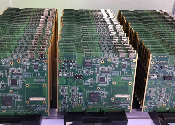
Our products are widely used in communication equipment, industrial control, consumer electronics, medical equipment, aerospace, light-emitting diode lighting, automotive electronics etc.
![]()
Workshop
![]()
![]()
![]()
1.PCB: Vacuum packaging with carton box
2.PCBA: ESD packaging with carton box
![]()
Our services cover all industries and reach all parts of the world.