Haina lean Electronics Co., Ltd is a one-stop EMS supplier integrating PCB design, PCB manufacturing, Component sourcing and PCB assembly.
Our company was established in May 1, 2012 in Beijing. And expansion was completed in June 2016. The company is specialized in electronic products supporting processing services, mainly to undertake circuit board design, layout production, components procurement, PCB plate making, circuit board welding assembly debugging and other OEM/ODM services.
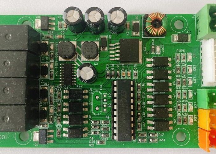
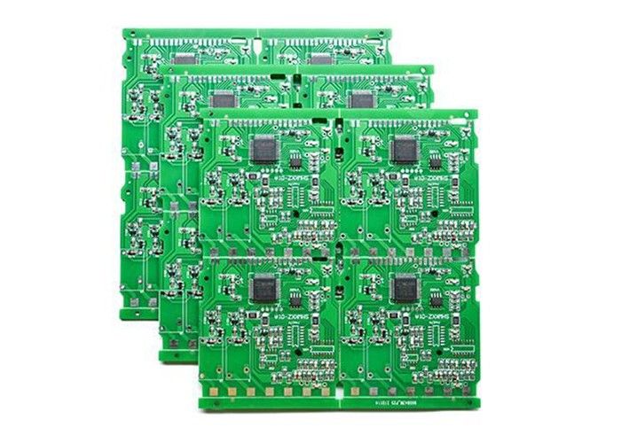
PCB'A short for printed circuit board assembly, refers to the combination of PCB, components and electronic accessories. In fact, PCBA is actually the PCB with components assembled.
| Factory Capabilities | |||
| Layers | 1-36 layers | Min Board Thickness | Core thickness 0..05-1.5mm ,Finished Board Thickness 0.3-3.5mm |
| Max Board Size | 700 × 610mm | Min Board Size | 20 × 30mm |
| Min Space | 0.03mm | Min Hole Location Tolerance | ±0.075mm |
| Min Hole Size | Laser 0.05 Mechnical 0.15mm | Min Hole Size Tolerance | ±0.05mm |
| Board Warp | 0.50% | Min Outer Dimension Tolerance | ±0.1mm |
| Solder Mask | Green, Yellow, Red, Black, Blue, White | ||
| Surface Finish | HASL Lead free, HASL, Immersion Gold, Immersion Silver, Plating Gold, Plating Nickel, Plating Silver, Gold Finger, OSP | ||
| Board Material | FR-4, High Tg FR-4, Halogen Free FR-4, Thick Copper FR-4, Aluminium Based, Rogers, Taconic | ||
| Acceptable file | Gerber file(RS-274-X or RS-274-D with aperture list and drill files),Protel,PADS,POWERPCB,AutoCAD,ORCAD | ||
| CAM software | Genesis, CAM350 | ||
| PCBA Capability | |||
| Material Type | Item | Min | Max |
| PCB | Dimension (length,width,height.mm) | 50*40*0.38 | 600*400*4.2 |
| Material | FR-4,CEM-1,CEM-3,Aluminium-based board,Rogers,ceramic plate,FPC | ||
| Surface finish | HASL,OSP,Immersion gold,Flash Gold Finger | ||
| Components | Chip&IC | 1005 | 55mm |
| BGA Pitch | 0.3mm | - | |
| QFP Pitch | 0.3mm | - | |
Types of PCB Assembly
Single-side SMD , Double-side SMD ,Single-side mixed assembly ,Mixed assembly on side A and simple SMD on side B ,Plug-in on Side A and simple SMD on side B
![]()
![]()
Material Distribution list, PCB manufacturing, SMT/DIP welding ,Test .
![]()
Our Advantages
Quick shipment
Imported ink
A grade raw materials
Fast service response
![]()
![]()
Turnkey PCB Assembly Application Field
Printed circuit boards And PCB Assembly are mainly used for many communication industry,aprospace,industrial control , medical equipments, consumer electronics ,automobile industry and smart home etc.![]()
![]()
![]()
PCB: Vacuum packaging with carton box
PCBA: ESD packaging with carton box
![]()
Company Information
Our first factory is located in Changping District, Beijing, the main radiation Haidian, Changping, Chaoyang three areas of Beijing. Since our company’s establishment, we have been adhering to creating high quality, high efficiency, low-cost business philosophy based on the circuit board processing industry for customers. Most of the key staff of the company are mature technical talents who have been engaged in the industry for more than 10 years, and have rich experience in the production of SMT and DIP, also has rich experience in production for high density & difficulty to package components such as BGA. The factory covers an area of 1500 square meters. Since its establishment, we obtain a good reputation in the industry through the continuous efforts of all staff and high quality service . Our second branch plant is located in Langfang city, and mainly cover Fengtai and Daxing Yizhuang area.
The company pursues "inclusiveness, excellence, people-oriented". Constantly innovate, take technology as the core, regard quality as life, and wholeheartedly provide customers with high-quality and high-efficiency humanized services.We are willing to serve our customers with the principle of continuous honesty & trustworthiness, pragmatism and innovation.
At present, the main cooperation industries are automotive electronics, communications, audio and video, optoelectronics, robotics, hydroelectric power, medical care, aerospace, education, radio frequency, power supply, printer etc industries.
![]()
Our services cover all industries and reach all parts of the world.