-
High Light
electronics fr4 pcba
,multilayer fr4 pcba
,communication multilayer pcba
-
Product NameFR4 Electronics Multilayer Custom Circuit PCBA For Communication
-
Copper Thickness1oz , 2oz ,3 Oz ..... 6oz
-
Layers1-36LAYERS
-
Min. Line Spacing0.030mm/0.030mm
-
Board Thickness0.3. 1.0mm .1.2mm 1.6mm ......3.5mm
-
TypePcb ,pcba , Box Assembly
-
Outline ProfileRout/ V-cut/ Bridge/ Stamp Hole
-
Solder Mask ColorGreen, White,Black. Blue(Customized)
-
CraftsmanshipHASL,HASL PB FREE,Immersion Gold/Tin/Silver, Gold Finger Plating OSP,Immersion Gold + OSP
-
ApplicationImage Processing ,video Processing ,communication Solutions ,automotive Electronics , Industry Control ,Medical
-
Place of OriginCHINA
-
Brand NameHNL-PCB
-
CertificationISO9001,IS16949, ISO14001,ROHS ,IPC-A ,QC080000
-
Model NumberFR4 Electronics Multilayer Custom Circuit PCBA For Communication
-
Minimum Order Quantity1 PC
-
PriceNegotiable
-
Packaging DetailsESD packaging with carton box
-
Delivery Time1-7days
-
Payment TermsT/T, Western Union, L/C, MoneyGram
-
Supply Ability10,000,000 Point /Day
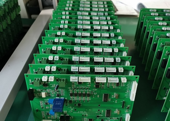
Electronics Multilayer Fr4 Pcba Custom Circuit For Communication

FR4 Electronics Multilayer Custom Circuit PCBA For Communication
Haina Lean is an OEM manufacturer that focus PCB Assembly (SMT ) manufacturing over 10 years. from double sided boards up to 36 layer multilayers ,and provide one stop turnkey services, including PCB layout, PCB assembly, components source, function testing services ,Box assembly and so on.
PCB CAPABILITIES
| No. | Items | |
| 1 | HDI Capabilities | HDI ELIC(5+2+5) |
| 2 | Max layer count | 36L |
| 3 | Board Thickness | Core thickness 0.05mm-1.5mm ,Fineshed board thickness0.3-3.5mm |
| 4 | Min.Hole Size | Laser 0.05mm |
| Mechnical 0.15 | ||
| 5 | Min Line Width/Space | 0.030mm/0.030mm |
| 6 | Copper Thickness | 1/3oz-6oz |
| 7 | Size Max Panel size | 700x610mm |
| 8 | Registration Accuracy | +/-0.05mm |
| 9 | Routing Accuracy | +/-0.05mm |
| 10 | Min.BGA PAD | 0.125mm |
| 11 | Max Aspect Ratio | 10:01 |
| 12 | Bow and Twist | 0.50% |
| 13 | Impedance Control Tolerance | +/-5% |
| 14 | Daily output | 4,000m2 (Max capacity of equipment) |
| 15 | Surface Finishing | ENEPING /ENIG /HASL /FINGER GOLD/IMMERSION TIN/SELECTIVE THICK GOLD |
| 16 | Raw Material | FR-4/Normal Tg/High Tg/Low Dk/HF FR4/PTEE/PI |
PCBA CAPABILITIES
| PCBA Capability | |||
| Material Type | Item | Min | Max |
| PCB | Dimension (length,width,height.mm) | 50*40*0.38 | 600*400*4.2 |
| Material | FR-4,CEM-1,CEM-3,Aluminium-based board,Rogers,ceramic plate,FPC | ||
| Surface finish | HASL,OSP,Immersion gold,Flash Gold Finger | ||
| Components | Chip&IC | 1005 | 55mm |
| BGA Pitch | 0.3mm | - | |
| QFP Pitch | 0.3mm | - | |
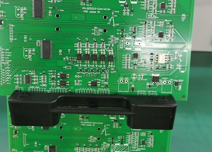
FR4 PCB Craftsmanship
Immersion gold ,Lead-free HASL,OSP,etc.
![]()
![]()
Our service
| Electronic Manufacturing Service | PCB Electronic Design |
| PCB Electronic Design | PCB Layout Service |
| PCB Assembly process service | PCBA Components Sourcing |
![]()
FR4 Printed Circuit Board Application Field
Printed circuit boards And PCB Assembly are mainly used for many communication industry, medical equipments, consumer electronics ,automotive electronics , audio and video, optoelectronics, robotics, hydroelectric power, aerospace, education, power supply, printer ,Auto Industry ,Smart Home.etc.
![]()
Workshop
![]()
![]()
![]()
![]()
Testing service
1. Manual visual inspection of PCB board
2. PCB board online test
3. PCB board function test
4. AOI (Automatic optical inspection)
5. Automatic X-ray inspection
6. Laser detection system
7. Size detection
Above is the PCB testing service.
Haina lean Electronics provides custom test service according to client's requirements and products.
Usually Haina lean Electronics Co.,Ltd PCBA Tech offers a full range of testing service. Including:
1. AOI(Automatic Optical Inspection)
2. Function Testing
3. In Circuit Testing
4. Testing Jig
5. Testing Service
6. X-Ray for BGA Testing
7. Printing Solder Paste Test
Each board is carefully examined by our dedicated inspection team using AOI and high magnification viewers.
Using our X-Ray machine, we test PCBs to component level and all wiring is fully inspected and tested.
Flash testing and earth bonding tests can also be undertaken where required.
![]()
Partners
![]()
Common packaging
PCB: Vacuum packaging with carton box
PCBA: ESD packaging with carton box
![]()
FAQ
Q1.What are needed for quoation ?
PCB :Gerber File (Protel.Power PCB ,PADs File)
PCBA: Gerber File and BOM
Q2.What file formats do you accept for production ?
Gerber file :CAM350 RS274X
PCB File:protel 99SE ,P-CAD 2001 PCB
BOM:Excel (PDF,Word ,txt)
Q3.Are my files safe ?
Your files are held in complete safety and security ,we protect the intellectual property for our customers in the whole process .All documents from customer are never shared with any third parties .
Q4.What's your MOQ ?
No Moq ,We small orders as well as mass production
Q5.Shipping Cost ?
The shipping cost is determined by the destination ,weight ,packing size of the goods .We can provide shipping, air, land, express and other transportation services .
Q6.Can You provide fast rotating PCB ?
Yes , we can provide fast service 24 hours .
Q7.What are the services you can provide ?
One-stop contract manufacturing
A:PCB Assembly;
B:PCB Design & Layout
C:PCBA programming & functional testing;
D:Electronic components purchasing service;
E:Enclosure molding & final assembly with labels,instructions,enclosure, boxes.
Q8.Whether all PCBA s will be tested before delivery ?
Yes , we will test each piece of PCBA product under your testing methods ,to ensure quality and functionality .
Q9.Do you provide OEM service ?
Yes ,we offer PCB and PCBA OEM Service , we manufacture the PCB and PCBA products to your design and requirements .
Company introduce
Beijing Haina lean Electronics Co.,Ltd is one of the most professional PCBA manufacture in Beijing,China. With more then 10 years of development, Haina Lean Electronics turns into a first class manufacture of HDI PCB ,with production capability 4000 square meters.
Our factory is providing high quality bare PCB, PCB layout design service and PCB assembly service,including components sourcing, function test,conformal coating and complete assembly for clients all.
Our services cover all industries and reach all parts of the world.