
Hdi Type Reflow Soldering Through Hole Pcb Assembly For Telecom
-
High Light
reflow soldering through hole pcb assembly
,hdi type through hole pcb assembly
,telecom pcb through hole assembly
-
Product NameHDI Type Reflow Soldering Thru-Hole PCB Assembly For Telecom
-
MaterialFR-4/Normal Tg/High Tg/Low Dk/HF FR4/ Aluminium
-
Layers1-36layers
-
Copper Thickness0.3oz-6oz
-
Min. Line Spacing0.030mm/0.030mm
-
Board Thickness0.3-3.5mm
-
Min. Line Width0.03mm
-
Min. Hole SizeLaser 0.05mm ; Mechnical 0.15
-
Surface FinishingHASL,OSP,ENIG,HASL Lead Free,Immersion Gold
-
Base MaterialHigh Tg FR-4, Halogen Free FR-4, Thick Copper FR-4, Aluminium Based, Rogers, Taconic
-
ApplicationIndustry/Medical/Telecom/Automotive
-
Solder Mask ColorGreen, Yellow, Red, Black, Blue, Whiteetc
-
Place of OriginCHINA
-
Brand NameHNL-PCBA
-
CertificationISO9001,IS16949, ISO14001,ROHS ,IPC-A ,QC080000
-
Model NumberPCB Assembly
-
Minimum Order Quantity1 PC
-
PriceNegotiable
-
Packaging DetailsESD packaging with carton box
-
Delivery Time1-7days
-
Payment TermsT/T, Western Union, L/C, MoneyGram
-
Supply Ability10,000,000 Point /Day
Hdi Type Reflow Soldering Through Hole Pcb Assembly For Telecom
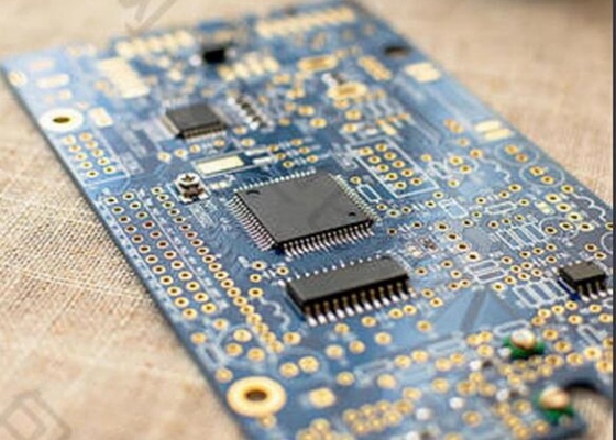

HDI Type Reflow Soldering Thru-Hole PCB Assembly For Telecom
Haina Lean technology is specialized in quick-turn, SMT assembly for design engineers needing low to mid-volume printed circuit board assembly.
Our production facility utilizes the latest technology and equipment, and we always keep tabs on industry trends and customer demands.
Here some of our quick turn PCB assembly capabilities:
Low to Mid-Volume Printed Circuit Board Assembly
Large Quantity Printed Circuit Board Assembly
SMT and Through-Hole Mounting
HDI Technology
Double-Sided SMT Assembly
RoHS-Compliant Circuit Boards
BGA Component Reballing
Factory Capabilities
| Factory Capabilities | |||
| Layers | 1-36 layers | Min Board Thickness | Core thickness 0..05-1.5mm ,Finished Board Thickness 0.3-3.5mm |
| Max Board Size | 700 × 610mm | Min Board Size | 20 × 30mm |
| Min Space | 0.03mm | Min Hole Location Tolerance | ±0.075mm |
| Min Hole Size | Laser 0.05 Mechnical 0.15mm | Min Hole Size Tolerance | ±0.05mm |
| Board Warp | 0.50% | Min Outer Dimension Tolerance | ±0.1mm |
| Solder Mask | Green, Yellow, Red, Black, Blue, White | ||
| Surface Finish | HASL Lead free, HASL, Immersion Gold, Immersion Silver, Plating Gold, Plating Nickel, Plating Silver, Gold Finger, OSP | ||
| Board Material | FR-4, High Tg FR-4, Halogen Free FR-4, Thick Copper FR-4, Aluminium Based, Rogers, Taconic | ||
| Acceptable file | Gerber file(RS-274-X or RS-274-D with aperture list and drill files),Protel,PADS,POWERPCB,AutoCAD,ORCAD | ||
| CAM software | Genesis, CAM350 | ||
PCBA CAPABILITIES
| PCBA Capability | |||
| Material Type | Item | Min | Max |
| PCB | Dimension (length,width,height.mm) | 50*40*0.38 | 600*400*4.2 |
| Material | FR-4,CEM-1,CEM-3,Aluminium-based board,Rogers,ceramic plate,FPC | ||
| Surface finish | HASL,OSP,Immersion gold,Flash Gold Finger | ||
| Components | Chip&IC | 1005 | 55mm |
| BGA Pitch | 0.3mm | - | |
| QFP Pitch | 0.3mm | - | |
Printed Circuit Board Assembly Order Process
Quotation information → confirm price → customer confirms order → customer information (purchasing materials)
Incoming inspection IQC→SMT Process→QC →reflow soldering→AOI/QC visual inspection (maintance)→DIP plug-in→QC →wave soldering→(solder repair)→QC→Assembly test (Functional maintenance)→QC appearance inspection→Packaging and shipping
![]()
Printed Circuit Board Assembly Technologies
SMT ,THT ,BGA ,HDI ,Reflow Soldering ,Wave Soldering ,Hand Soldering ,Repair/Rework ,Mixed Assembly Technologies .
![]()
![]()
![]()
![]()
Delivery Time
| Product Type | Qty | Normal lead time | Quick-turn lead time |
| SMT+DIP | 1-50 | 1WD-2WD | 8H |
| SMT+DIP | 51-200 | 2WD-3WD | 1.5WD |
| SMT+DIP | 201-2000 | 3WD-4WD | 2WD |
| SMT+DIP | ≥2001 | 4WD-5WD | 3WD |
| PCBA(2-4Layer) | 1-50 | 2.5WD-3.5WD | 1WD |
| PCBA(2-4Layer) | 51-2000 | 5WD-6WD | 2.5WD |
| PCBA(2-4Layer) | ≥2001 | ≥7WD | 5WD |
| PCBA(6-10Layer) | 1-50 | 3WD-4WD | 2.5WD |
| PCBA(6-10Layer) | 51-2000 | 7WD-8WD | 6WD |
| PCBA(10-HDILayer) | 1-50 | 7WD-9WD | 5WD |
| PCBA(10-HDILayer) | 51-2000 | 9WD-11WD | 7WD |
Printed Circuit Board Assembly Application Field
1. Industrial control equipment
2. Security equipment
3. Automotive electronics
4. Solar
5. Wireless charging
6. Internet of Things
7. Consumer electronics
8. Medical equipment
![]()
Partners
![]()
Common packaging
PCB: Vacuum packaging with carton box
PCBA: ESD packaging with carton box
![]()
Certification
![]()
FAQ
Q1.What are needed for quoation ?
PCB :Gerber File (Protel.Power PCB ,PADs File)
PCBA: Gerber File and BOM
Q2.What file formats do you accept for production ?
Gerber file :CAM350 RS274X
PCB File:protel 99SE ,P-CAD 2001 PCB
BOM:Excel (PDF,Word ,txt)
Q3.Are my files safe ?
Your files are held in complete safety and security ,we protect the intellectual property for our customers in the whole process .All documents from customer are never shared with any third parties .
Q4.What's your MOQ ?
No Moq ,We accept small orders as well as mass production
Q5.Shipping Cost ?
The shipping cost is determined by the destination ,weight ,packing size of the goods .We can provide shipping, air, land, express and other transportation services .
Q6.Can You provide fast rotating PCB ?
Yes , we can provide fast service 24 hours .
Q7.What are the services you can provide ?
One-stop contract manufacturing
A:PCB Assembly;
B:PCB Design & Layout
C:PCBA programming & functional testing;
D:Electronic components purchasing service;
E:Enclosure molding & final assembly with labels,instructions,enclosure, boxes.
Q8.Whether all PCBA s will be tested before delivery ?
Yes , we will test each piece of PCBA product under your testing methods ,to ensure quality and functionality .
Q9.Do you provide OEM service ?
Yes ,we offer PCB and PCBA OEM Service , we manufacture the PCB and PCBA products to your design and requirements .
Our services include
![]()
Company Information
Haina lean Electronics Co., Ltd is a one-stop EMS supplier integrating PCB design, PCB manufacturing, Component sourcing and PCB assembly.
Our company was established in May 1, 2012 in Beijing. And expansion was completed in June 2016. The company is specialized in electronic products supporting processing services, mainly to undertake circuit board design, layout production, components procurement, PCB plate making, circuit board welding assembly debugging and other OEM/ODM services.
At present, the main cooperation industries are automotive electronics, communications, audio and video, optoelectronics, robotics, hydroelectric power, medical care, aerospace, education, radio frequency, power supply, printer etc industries.
![]()
Our services cover all industries and reach all parts of the world.