-
High Light
odm pcb smt assembly
,pcb smt assembly 2 layer
,hasl lead free smt circuit board
-
Product NamePCB SMT Assembly
-
MaterialFr4 Common Tg; High Tg
-
Copper Thickness1OZ To 6OZ
-
Min. Line Width/spacing0.030mm
-
Board Thickness0.5mm, 1.6mm,...... 3.5mm
-
Min. Hole SizeLaser 0.05mm ; Mechnical 0.15
-
Surface FinishingHASL Lead Free
-
Solder Mask ColorGreen. Red. Blue. White. Black.Yellow Etc.
-
ServiceOne-stop Service,PCB&PCBA,ODM And OEM
-
PCB Assembly MethodMixed; SMT, DIP, THT
-
Place of OriginCHINA
-
Brand NameHNL-PCBA
-
CertificationISO9001,IS16949, ISO14001,ROHS ,IPC-A ,QC080000
-
Model NumberPCB Assembly 04
-
Minimum Order Quantity1 PC
-
PriceNegotiable
-
Packaging DetailsESD packaging with carton box
-
Delivery Time1-10days
-
Payment TermsT/T, Western Union, L/C, MoneyGram
-
Supply Ability10,000,000 Point /Day
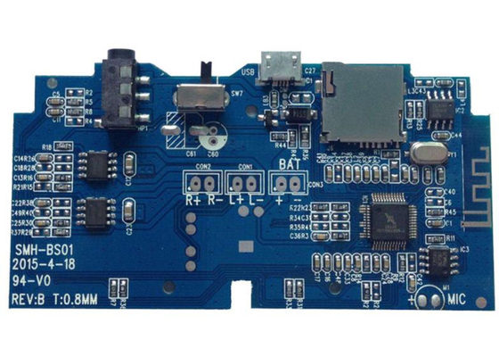
ODM Hasl Lead Free Pcb Smt Assembly 2 Layer 0.6oz


HASL Lead Free 2layer 0.6oz Electronic Circuit PCB SMT Assembly
PCB SMT Assembly Introduction
SMT development trend:
Higher process stability and reliability to meet mass production, professional production, reduce costs.
Higher assembly precision, to meet the micro-spacing device mounting, improve assembly density.
Higher technical content, adapt to the assembly of new device packaging.
It is conducive to environmental protection and human health.
We offer competitive pricing, as well as flexible shipment plans to you. Our engineers is qualified and experienced in producing surface-mount (SMT), through-hole (THT) and mixed-technology components and fine-pitch parts and ball grid arrays (BGAs) for high-density FR-4 PCBs .
PCB CAPABILITIES
| Layers | 1 - 46 L (Custom ) |
| Substrate | FR-4,CTI600,Tg180,,Anti CAF,Halogen-free,,High frequency,Tg170&HF |
| Max. panel size | 700x610mm (Custom) |
| Board thickness | 0.3 mm - 3.5 mm. |
| Copper thickness | 1/3 oz. to 6 oz. (outer) (Max) |
| Hole | > 0.15mm. |
| Aspect Ratio | 10 : 1 |
| Min. track width | 3.0 mils(partial) |
| Min. track space | 3.0mils(partial) |
| Min. S/M bridge | 3mil |
| Hole plugging diameter | 0.3 mm~0.55 mm. |
| Impedance tolerance | +/- 10%. |
| Color of S/M | green,white,black,red,orange,yellow,blue,purple |
| Surface treatment | OSP,HAL,HAL LF,ENIG,Hard gold,Imm Ag,Imm Sn,Peelable soldermask,Carbon ink print,Selective hard gold |
PCBA CAPABILITIES
| PCBA Capability | |||
| Material Type | Item | Min | Max |
| PCB | Dimension (length,width,height.mm) | 50*40*0.38 | 600*400*4.2 |
| Material | FR-4,CEM-1,CEM-3,Aluminium-based board,Rogers,ceramic plate,FPC | ||
| Surface finish | HASL,OSP,Immersion gold,Flash Gold Finger | ||
| Components | Chip&IC | 1005 | 55mm |
| BGA Pitch | 0.3mm | - | |
| QFP Pitch | 0.3mm | - | |
Our SMT capabilities:
SMT Assembly: SMT provides a flexible high technology. These solutions include:
7 high-speed placement machines,
7 automatic printers with fiducial alignment,
2 X-ray machines,
BGA maintenance machines,
ICT test machines
Our DIP function:
A-8 semi-assembly production line with four wave soldering machines
1 U-shaped automatic assembly line for box-type building products with test stations
High temperature / low temperature aging test furnace B-4 for products required for aging test
With time control and temperature control
All products are 100% inspected and tested during the DIP process
Haina lean Electronics Co.,Ltd is a competitive China customize pcba for medical breathing machine OEM manufacturer, supplier and vendor, you can get quick turn customize pcba for medical breathing machine production prototypes and samples from our factory.
Hot Tags: customize pcba for medical breathing machine, China, supplier, manufacturer, factory, OEM manufacturer, vendor, samples, production, prototypes, quick turn
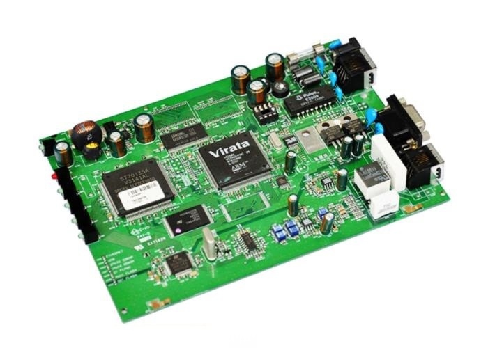
PCB SMT Assembly Process
1.Solder Paste stenciling---2.Surface Mount Technology (Pick and Place)---3.Reflow Soldering---4.Inspection and Quality Control---5.Through-Hole Component Insertion (DIP Process)---6.Final Inspection and Functional Test
![]()
Our advantage
1.Service value
Independent quotation system to quickly serve the market
2.PCB manufacturing
High-tech PCB and PCB assembly production line
3.Material purchasing
A team of experienced electronic component procurement engineers
4.SMT post soldering
Dust-free workshop, high-end SMT patch processing
![]()
![]()
PCB SMT Assembly Delivery Time
| Product Type | Qty | Normal lead time | Quick-turn lead time |
| SMT+DIP | 1-50 | 1WD-2WD | 8H |
| SMT+DIP | 51-200 | 2WD-3WD | 1.5WD |
| SMT+DIP | 201-2000 | 3WD-4WD | 2WD |
| SMT+DIP | ≥2001 | 4WD-5WD | 3WD |
| PCBA(2-4Layer) | 1-50 | 2.5WD-3.5WD | 1WD |
| PCBA(2-4Layer) | 51-2000 | 5WD-6WD | 2.5WD |
| PCBA(2-4Layer) | ≥2001 | ≥7WD | 5WD |
| PCBA(6-10Layer) | 1-50 | 3WD-4WD | 2.5WD |
| PCBA(6-10Layer) | 51-2000 | 7WD-8WD | 6WD |
| PCBA(10-HDILayer) | 1-50 | 7WD-9WD | 5WD |
| PCBA(10-HDILayer) | 51-2000 | 9WD-11WD | 7WD |
Electronic Board Assembly Application Field
Our products are widely used in
1.communication equipment,
2.industrial control,
3.consumer electronics,
4.medical equipment,
5.aerospace,
6.light-emitting diode lighting,
7.automotive electronics etc.
![]()
Workshop
![]()
![]()
![]()
Common packaging
1.PCB: Vacuum packaging with carton box
2.PCBA: ESD packaging with carton box
![]()
FAQ
1.What are needed for quotation?
PCB: Quantity, Gerber file and Technic requirements(material,surface finish treatment, copper thickness,board thickness ......)
PCBA: PCB information, BOM, (Testing documents...)
2. What file formats do you accept for production?
Gerber file: CAM350 RS274X
PCB file: Protel 99SE, P-CAD 2001 PCB
BOM: Excel (PDF,word,txt)
3.Are my files safe?
Your files are held in complete safety and security.We protect the intellectual property for our customers in the whole process.. All documents from customers are never shared with any third party.
4.MOQ?
There is no MOQ .We can flexibly handle small and mass production.
5.Shipping Cost ?
The shipping cost is determined by the destination ,weight ,packing size of the goods .We can provide shipping, air, land, express and other transportation services .
6.How to ensure high-quality production?
The process is strictly controlled under ISO 9001:2015 standards.
Most of our advanced equipment and tools are imported from abroad. Such as Flying Probe, X-ray Inspection, AOI (Automated Optical Inspector) and ICT (in-circuit testing).
We have a very professional QC team.
Company Information
Haina lean Electronics Co., Ltd is a one-stop EMS supplier integrating PCB design, PCB manufacturing, Component sourcing and PCB assembly.
We have profuse experience in manufacturing PCB,owned experienced technical R & D technology team, young and professional sales and customer service team, experienced and professional procurement team and assembly testing team, which make sure the products quality of the pass rate, on-time delivery rate of customer orders. The company is specialized in electronic products supporting processing services, mainly to undertake circuit board design, layout production, components procurement, PCB plate making, circuit board welding assembly debugging and other OEM/ODM services.
![]()
Our services cover all industries and reach all parts of the world.