-
High Light
1.6mm Rigid Flexible PCB
,HDI Rigid Flexible PCB
,4oz Rigid Flex Board
-
Product NameRigid Flexible PCB
-
LayersCustom
-
Copper Thickness0.3oz 1oz 2oz 3oz ..... 6oz
-
Min. Line Spacing0.030mm/0.030mm
-
Board Thickness0.3.0.6.1.2 1.6 ......3.5mm
-
Solder Mask ColorGreen, White,Black. Blue (Customized)
-
ServicePCB Fabrication /PCB Design / FCB / FPCB / PCBA
-
Base MaterialHigh Tg FR-4, Halogen Free FR-4, Thick Copper FR-4, Aluminium Based, Rogers, Taconic
-
Surface FinishingHASL Lead Free,HASL,OSP,ENIG,Immersion Gold ,Immersion Tin ,FINGER GOLD
-
ApplicationCommunication Industry, Power, Security, Optoelectronics, Industrial Control, Medical Equipments
-
Place of OriginCHINA
-
Brand NameHNL-PCB
-
CertificationISO9001,IS16949, ISO14001,ROHS ,IPC-A ,QC080000
-
Model NumberRigid Flexible PCB
-
Minimum Order Quantity1 PC
-
PriceNegotiable
-
Packaging DetailsESD packaging with carton box
-
Delivery Time1-7days
-
Payment TermsT/T, Western Union, L/C, MoneyGram
-
Supply Ability10,000,000 Point /Day
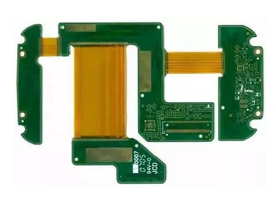
High Precision Blind Buried Via HDI Rigid Flexible PCB

High Precision Multilayer Blind and Buried Via Rigid Flexible HDI Rigid Flexible PCB
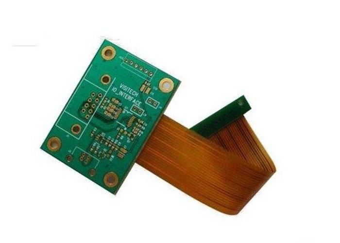
The rigid-flex board is the flexible circuit board and the rigid circuit board, referred to as FPCB. After pressing and other processes, they are combined according to the relevant process requirements to form a circuit board with FPC characteristics and PCB characteristics.
It can be used in some products with special requirements. It has both a certain flexible area and a certain rigid area. It is of great help to save the internal space of the product, reduce the volume of the finished product, and improve the performance of the product.
Haina Lean Electronics is providing high quality bare PCB,PCB layout design service ,FPC (flexible PCB) ,FPCB (Rigid flexible PCB ) and PCB assembly service (Rapid PCBA ),including components sourcing, function test,conformal coating and complete assembly for clients all.
Factory capabilities
| Quality Grade | Standard IPC 2 | Material | FR-4/Normal Tg/High Tg/Low Dk/HF FR4/PTEE/PI |
| Number of Layers | 1 - 8layers | Board Size | Custom |
| Order Quantity | 1pc - 10000+pcs | Board Thickness | 0.1mm - 0.8mm |
| Build Time | 2days - 5weeks | Copper Weight (Finished) | 0.5oz - 6.0oz |
| Min Tracing/Spacing | 3mil/3mil | Silkscreen Sides | As per the file |
| Solder Mask Sides | As per the file | Silkscreen Color | White, Black, Yellow |
| Solder Mask Color | Green, White, Blue, Black, Red, Yellow | Surface Finish | HASL - Hot air solder leveling |
| Solder-stop coating---Soldermask oil | Green, White, Blue, Black, Red, Yellow | Lead - free HASL - RoHS | |
| Solder-stop coating---Coverlay | PI and PET film | ENIG - RoHS | |
| Min Annular Ring | 3mil | Immersion Tin - RoHS | |
| Min Drilling Hole Diameter | 8mil | OSP - RoHS | |
| Min. hole size---Drilling (PTH) | 0.2mil | Other Techniques | Peelable solder mask ;Gold fingers ;Stiffener (only for PI/FR4 substrate) |
Process flow
1 Material selection
2 Production process flow and control of key parts
2.1 Production process
2.2 Graphic transfer of the inner monolithic
2.3 Multi-layer positioning of flexible materials
2.4 Laminating
2.5 Drilling
2.6 De-drilling and protruding corrosion
2.7 Electroless copper plating, copper electroplating
2.8 Surface solder mask and solderability protective layer
2.9 Shape processing
![]()
Our service
Electronic Manufacturing Service
PCB Electronic Design
PCB Layout Service
PCB Supplier & Quality Inspection Service
PCBA Components Sourcing
PCB Assembly process service
Our advantages
1. Our company has passed the ISO2001 quality system certification, and the processed products meet the export standards of Europe and America
2. There is no minimum order quantity limit, which supports the whole process from sample to batch.
3. A professional component procurement team, centralized procurement, to save your procurement costs, labor costs, quality costs.
4. Professional sample making: SMT samples will be delivered within 24 hours.
5. Our main customer base: automotive electronics, industrial control, security, communication, power and other high-end.
Delivery Time of PCB board
1. PCB production time: sample: 3-4 days / production: within 7 days
2. Fast pcb delivery: 24 hours for 2L ; 48 hours for 4L ; 72 hours for 6L.
3. Component purchase: 2 days if all components is available in our domestic market. PCB Assembly: samples: within 8 days / mass production: within 12 days
| Prototype PCB | Batch | Prototype | Expedited |
| Double sides | 9 Days | 5 Days | 45h |
| Four-layer | 10 Days | 5 Days | 3 Days |
| Six-layer | 12 Days | 6 Days | 3 Days |
| Eight-layer | 12 Days | 7 Days | 4 Days |
| Ten-layer | 14 Days | 10 Days | 4Days |
| Twelve-layer | 14 Days | 10 Days | 5 Days |
| Fourteen-layer | 16 Days | 12Days | 6 Days |
| Sixteen-layer | 16 Days | 12 Days | 6 Days |
| Eighteen-layer | 18 Days | 14 Days | 6 Days |
| Twenty-layer | 18 Days | 14 Days | 10 Days |
| Twenty two-layer | 20 Days | 14 Days | 10 Days |
| Twenty four-layer | 20 Days | 14 Days | 10 Days |
| Twenty six-layer | 20 Days | 14 Days | 10 Days |
| Twenty eight-layer | 20 Days | 14 Days | 10 Days |
Rigid Flexible PCB Application Field
Printed circuit boards and PCB Assembly are widey used in communication industry, power, security, optoelectronics, industrial control, medical equipments, consumer electronics and automobile industry etc field.
![]()
Workshop
![]()
![]()
![]()
![]()
Testing service
1. Manual visual inspection of PCB board
2. PCB board online test
3. PCB board function test
4. AOI (Automatic optical inspection)
5. Automatic X-ray inspection
6. Laser detection system
7. Size detection
Above is the PCB testing service.
Usually Haina lean Electronics Co.,Ltd PCBA Tech offers a full range of testing service. Including:
1. AOI(Automatic Optical Inspection)
2. Function Testing
3. In Circuit Testing
4. Testing Jig
5. Testing Service
6. X-Ray for BGA Testing
7. Printing Solder Paste Test
Each board is carefully examined by our dedicated inspection team using AOI and high magnification viewers.
Using our X-Ray machine, we test PCBs to component level and all wiring is fully inspected and tested.
Flash testing and earth bonding tests can also be undertaken where required.
Partners
![]()
Common packaging
PCB: Vacuum packaging with carton box
PCBA: ESD packaging with carton box
![]()
Why choose us?
Welcome to visit our factory, Haina lean Electronics Co., Ltd.
1. Experienced: Focus on PCB And PCBA munufacturing over 10 years.
2. Professional: Expertise engineer with barrier-free English
3. Rapid delivery: On-time delivery rate reaches 98%
4.Cost effective: No excessive profits. Lower cost with same quality And service
![]()
Our services cover all industries and reach all parts of the world.