-
High Light
ENIG PCB substrate FR4
,HASL PCB substrate FR4
,3oz FR4 PCB sheet
-
Product NameFR4 Printed Circuit Board
-
Copper Thickness0.3oz 1oz 2oz 3oz ..... 6oz
-
Layers1-36 Layers (Custom)
-
Finished Board Thickness0.3mm 1.2mm 1.6mm ......3.5mm
-
Min. Line Spacing0.030mm/0.030mm
-
Min. Hole SizeLaser 0.05mm ; Mechnical 0.15
-
TypePrinting Circuit Board,PCBA Design
-
Solder Mask ColorGreen, White,Black. Blue(Customized)
-
Acceptable FileAcceptable File,Protel,PADS,POWERPCB,AutoCAD,ORCAD
-
ServicePCB/PCBA/Circuit Board/SMT/DIP PCBA Layout And Design
-
CraftsmanshipHASL,HASL PB FREE, Immersion Gold/Tin/Silver, Gold Finger Plating OSP,Immersion Gold + OSP
-
ApplicationCommunication Industry, Medical Equipments, Consumer Electronics ,automotive Electronics Etc
-
Place of OriginCHINA
-
Brand NameHNL-PCB
-
CertificationISO9001,IS16949, ISO14001,ROHS ,IPC-A ,QC080000
-
Model NumberFR4 Printed Circuit Board
-
Minimum Order Quantity1 PC
-
PriceNegotiable
-
Packaging DetailsESD packaging with carton box
-
Delivery Time1-7days
-
Payment TermsT/T, Western Union, L/C, MoneyGram
-
Supply Ability10,000,000 Point /Day
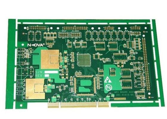
ENIG HASL Prototype Board Soldering PCB Substrate FR4

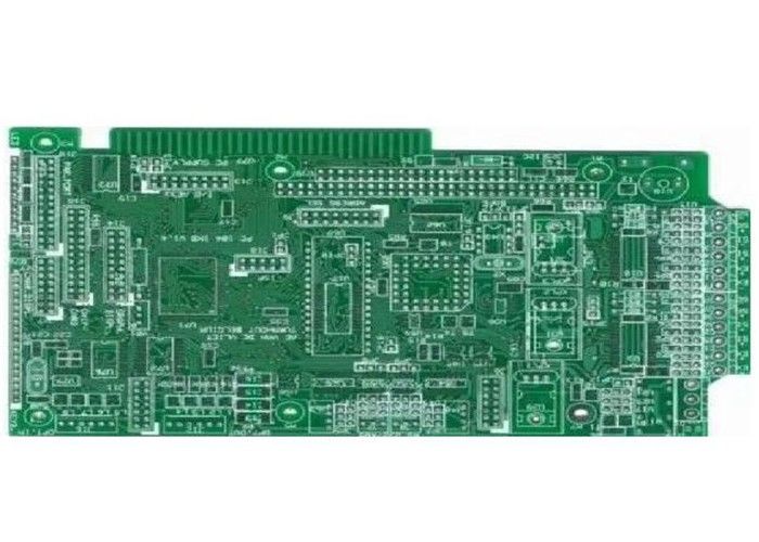
ENIG HASL Prototype Board Soldering Multilayer FR4 Printed Circuit Board
FR4 Printed Circuit Board Introduction
Printed Circuit Boards include Single-layer, Double-layer, Multi-layer, Rigid Board, Rigid-flexible Board, Flexible Board, High Frequency Board,
HDI PCB board, Aluminum Substrate .
Haina lean Electronics is a one-stop EMS supplier integrating PCB design, PCB manufacturing, Component sourcing and PCB assembly.
The company is specialized in electronic products supporting processing services, mainly to undertake circuit board design, layout production, components procurement, PCB plate making, circuit board welding assembly debugging and other OEM/ODM services.
PCB Capabilities
| FACTORY CAPABILITIES | |||
| No. | Items | 2019 | 2020 |
| 1 | HDI Capabilities | HDI ELIC (4+2+4) | HDI ELIC(5+2+5) |
| 2 | Max layer count | 32L | 36L |
| 3 | Board Thickness | Core thickness 0.05mm-1.5mm ,Fineshed board thickness 0.3-3.5mm | Core thickness 0.05mm-1.5mm ,Fineshed board thickness 0.3-3.5mm |
| 4 | Min.Hole Size | Laser 0.075mm | Laser 0.05mm |
| Mechnical 0.15mm | Mechnical 0.15mm | ||
| 5 | Min Line Width/Space | 0.035mm/0.035mm | 0.030mm/0.030mm |
| 6 | Copper Thickness | 1/3oz-4oz | 1/3oz-6oz |
| 7 | Size Max Panel size | 700x610mm | 700x610mm |
| 8 | Registration Accuracy | +/-0.05mm | +/-0.05mm |
| 9 | Routing Accuracy | +/-0.075mm | +/-0.05mm |
| 10 | Min.BGA PAD | 0.15mm | 0.125mm |
| 11 | Max Aspect Ratio | 10:1 | 10:1 |
| 12 | Bow and Twist | 0.50% | 0.50% |
| 13 | Impedance Control Tolerance | +/-8% | +/-5% |
| 14 | Daily Output | 3,000m2 (Max capacity of equipment) | 4,000m2 (Max capacity of equipment) |
| 15 | Surface Finishing | ENEPING /ENIG /HASL /FINGER GOLD/IMMERSION TIN/SELECTIVE THICK GOLD | |
| 16 | Raw Material | FR-4/Normal Tg/High Tg/Low Dk/HF FR4/PTEE/PI | |
FR4 PCB Craftsmanship
Immersion gold ,Lead-free HASL,OSP,etc.
![]()
![]()
Our service
| Electronic Manufacturing Service | PCB Electronic Design |
| PCB Electronic Design | PCB Layout Service |
| PCB Assembly process service | PCBA Components Sourcing |
![]()
FR4 Printed Circuit Board Application Field
Printed circuit boards And PCB Assembly are mainly used for many communication industry, medical equipments, consumer electronics ,automotive electronics , audio and video, optoelectronics, robotics, hydroelectric power, aerospace, education, power supply, printer ,Auto Industry ,Smart Home.etc.
![]()
Workshop
![]()
![]()
![]()
![]()
Testing service
1. Manual visual inspection of PCB board
2. PCB board online test
3. PCB board function test
4. AOI (Automatic optical inspection)
5. Automatic X-ray inspection
6. Laser detection system
7. Size detection
Above is the PCB testing service.
Haina lean Electronics provides custom test service according to client's requirements and products.
Usually Haina lean Electronics Co.,Ltd PCBA Tech offers a full range of testing service. Including:
1. AOI(Automatic Optical Inspection)
2. Function Testing
3. In Circuit Testing
4. Testing Jig
5. Testing Service
6. X-Ray for BGA Testing
7. Printing Solder Paste Test
Each board is carefully examined by our dedicated inspection team using AOI and high magnification viewers.
Using our X-Ray machine, we test PCBs to component level and all wiring is fully inspected and tested.
Flash testing and earth bonding tests can also be undertaken where required.
Partners
![]()
Common packaging
PCB: Vacuum packaging with carton box
PCBA: ESD packaging with carton box
![]()
Why choose us?
Welcome to visit our factory, Haina lean Electronics Co., Ltd.
1. Experienced: Focus on PCB And PCBA munufacturing over 10 years.
2. Professional: Expertise engineer with barrier-free English
3. Rapid delivery: On-time delivery rate reaches 98%
4.Cost effective: No excessive profits. Lower cost with same quality And service
![]()
Our services cover all industries and reach all parts of the world.