
-
High Light
5oz HDI PCB Board
,Immersion Gold HDI PCB Board
,HDI 2 layer PCB board
-
Product NameHDI PCB Board
-
Layers1-36 Layers (Custom)
-
Copper Thickness1/3oz-6oz
-
Min. Line Spacing0.030mm/0.030mm
-
Board Thickness0.3-3.5mm
-
Solder Mask ColorGreen, Yellow, Red, Black, Blue, White Etc
-
Surface FinishingHASL ,Lead Free HASL,ENIG ,Immersion Silver,Immersion Tin,OSP
-
MaterialFR4 Standard Tg 140°C,FR4 High Tg 170°C, FR4 And Rogers Combined Lamination
-
ApplicationAutomotive , Aerospace Industries,medical Devices,Industrial Automation, In Automobiles, Aircraft , Touch-screen Devices, 4/5G Network Communications, Military Applications , Avionics , Smart Munitions
-
Advantage1.High Component Density 2.Space-saving 3.Lightweight Boards 4.Fast Processing 5.Save Number Of Layers 6.Accommodate Low Pitch Packages 7.High Reliability
-
Place of OriginCHINA
-
Brand NameHNL-PCBA
-
CertificationISO9001,IS16949, ISO14001,ROHS ,IPC-A ,QC080000
-
Model NumberHDI PCB Board
-
Minimum Order Quantity1 PC
-
PriceNegotiable
-
Packaging DetailsESD packaging with carton box
-
Delivery Time1-7days
-
Payment TermsT/T, Western Union, L/C, MoneyGram
-
Supply Ability10,000,000 Point /Day
Immersion Gold 2 Layer 4 Layer HDI PCB Board Higher Wiring Density
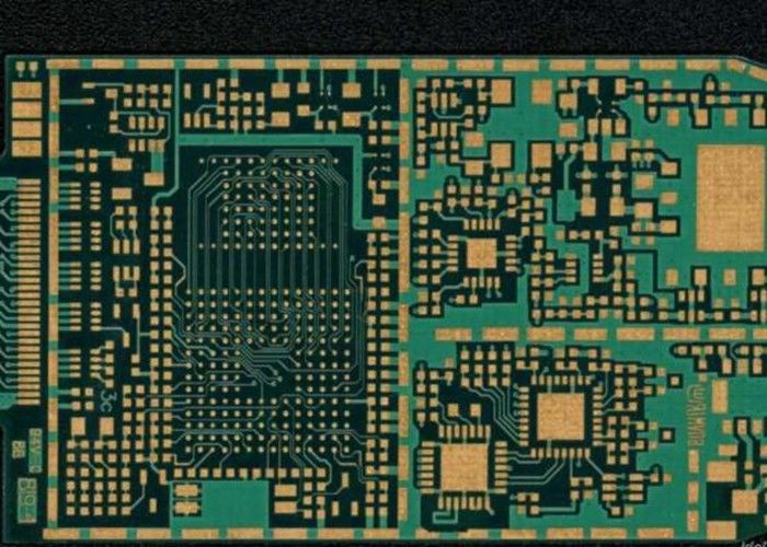
Immersion Gold 2 LAYER PCB 4 Layers Higher Wiring Density FR4 HDI PCB Board
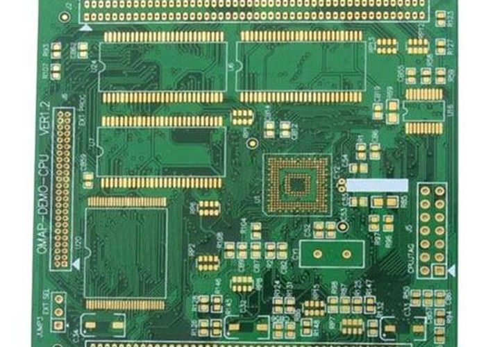
HDI PCB Board Introduction
HDI PCB Board also known as high-density interconnect PCB, is a kind of PCB with a higher wiring density per unit area than traditional boards. HDI boards are more compact and have smaller vias, pads, copper traces and spaces. As a result, HDIs have denser wiring resulting in lighter weight, more compact, lower layer count PCBs. HDI PCB is more fit into the little spaces and have a smaller amount of mass than conservative PCB designs.
Haina lean Electronics is a one-stop EMS supplier integrating PCB design, PCB manufacturing, Component sourcing and PCB assembly.
The company is specialized in electronic products supporting processing services, mainly to undertake circuit board design, layout production, components procurement, PCB plate making, circuit board welding assembly debugging and other OEM/ODM services.
PCB CAPABILITIES
| FACTORY CAPABILITIES | |||
| No. | Items | 2019 | 2020 |
| 1 | HDI Capabilities | HDI ELIC (4+2+4) | HDI ELIC(5+2+5) |
| 2 | Max layer count | 32L | 36L |
| 3 | Board Thickness | Core thickness 0.05mm-1.5mm ,Fineshed board thickness 0.3-3.5mm | Core thickness 0.05mm-1.5mm ,Fineshed board thickness 0.3-3.5mm |
| 4 | Min.Hole Size |
Laser 0.075mm Mechnical 0.15 |
Laser 0.05mm Mechnical 0.15 |
| 5 | Min Line Width/Space | 0.035mm/0.035 | 0.030mm/0.030mm |
| 6 | Copper Thickness | 1/3oz-4oz | 1/3oz-6oz |
| 7 | Size Max Panel size | 700x610mm | 700x610mm |
| 8 | Registration Accuracy | +/-0.05mm | +/-0.05mm |
| 9 | Routing Accuracy | +/-0.075mm | +/-0.05mm |
| 10 | Min.BGA PAD | 0.15mm | 0.125mm |
| 11 | Max Aspect Ratio | 10:1 | 10:1 |
| 12 | Bow and Twist | 0.50% | 0.50% |
| 13 | Impedance Control Tolerance | +/-8% | +/-5% |
| 14 | Daily output | 3,000m2 (Max capacity of equipment) | 4,000m2 (Max capacity of equipment) |
| 15 | Surface Finishing | HASL Lead Free /ENEPING /ENIG /HASL /FINGER GOLD/IMMERSION TIN/SELECTIVE THICK GOLD | |
| 16 | Raw Material | FR-4/Normal Tg/High Tg/Low Dk/HF FR4/PTEE/PI | |
PCBA CAPABILITIES
| PCBA Capability | |||
| Material Type | Item | Min | Max |
| PCB | Dimension (length,width,height.mm) | 50*40*0.38 | 600*400*4.2 |
| Material | FR-4,CEM-1,CEM-3,Aluminium-based board,Rogers,ceramic plate,FPC | ||
| Surface finish | HASL,OSP,Immersion gold,Flash Gold Finger | ||
| Components | Chip&IC | 1005 | 55mm |
| BGA Pitch | 0.3mm | - | |
| QFP Pitch | 0.3mm | - | |
The types of HDI PCB
1.through vias from surface to surface,
2.with buried vias and through vias,
3.two or more HDI layer with through vias,
4.passive substrate with no electrical connection,
5.coreless construction using layer pairs
6.alternate constructions of coreless constructions using layer pairs.
![]()
Work flow for HDI
Board Cut - Inner Wet film -DES - AOI - Brown Oxido - Outer Layer Press - Out Layer Lamination - X-RAY & Rounting - Copper reduce & brown oxide - Laser Drilling - Drilling - Desmear PTH - Panel plating - Outer Layer dry film - Etching - AOI- Impedance Testing - S/M Pluged hole - Solder Mask - Component Mark - Impedance testing - Immersion Gold -V-cut - Routing - Electrical Test - FQC - FQA -Package -Shipment
![]()
Our Service
| 1.PCB design: we can provide circuit design & PCB layout support. |
5.Component procurement: we have rich experience purchasing & material control expertise team. |
| 2.SMT Assembly: Leading edge surface mount population technologies. |
6.Complete turnkey solutions |
| 3.PTH Assembly: RoHS compliant wave soldering & hand soldering capabilities. |
7.Function Test & Inspection: |
| 4.PCB Fabrication: You only need provide Gerber files or other design files . |
8.We offer test & inspection services on PCB & Assembly (X-ray,ICT, AOI and Functional tests) |
![]()
WorkShop
![]()
Advantages of HDI PCB
1.High Component Density
2.Space-saving
3.Lightweight Boards
4.Fast Processing
5.Save Number of Layers
6.Accommodate Low Pitch Packages
7.High Reliability
HDI PCB Application Field
HDI PCB board are mainly used for many industries , Like : Automotive ; aerospace industries;medical devices;Industrial automation,etc .
Except mentioned above, you'll also can find high-density interconnect PCBs in all types of digital devices, like smartphones and tablets, in automobiles, aircraft , mobile /cellular phones, touch-screen devices, laptop computers, digital cameras, 4/5G network communications, and military applications such as avionics and smart munitions.
Partners
![]()
Common packaging
PCB: Vacuum packaging with carton box
PCBA: ESD packaging with carton box
![]()
FAQ
Q1.What are needed for quoation ?
PCB :Gerber File (Protel.Power PCB ,PADs File)
PCBA: Gerber File and BOM
Q2.What file formats do you accept for production ?
Gerber file :CAM350 RS274X
PCB File:protel 99SE ,P-CAD 2001 PCB
BOM:Excel (PDF,Word ,txt)
Q3.Are my files safe ?
Your files are held in complete safety and security ,we protect the intellectual property for our customers in the whole process .All documents from customer are never shared with any third parties .
Q4.What's your MOQ ?
No Moq ,We small orders as well as mass production
Q5.Shipping Cost ?
The shipping cost is determined by the destination ,weight ,packing size of the goods .We can provide shipping, air, land, express and other transportation services .
Q6.Can You provide fast rotating PCB ?
Yes , we can provide fast service 24 hours .
Q7.What are the services you can provide ?
One-stop contract manufacturing
A:PCB Assembly;
B:PCB Design & Layout
C:PCBA programming & functional testing;
D:Electronic components purchasing service;
E:Enclosure molding & final assembly with labels,instructions,enclosure, boxes.
Q8.Whether all PCBA s will be tested before delivery ?
Yes , we will test each piece of PCBA product under your testing methods ,to ensure quality and functionality .
Q9.Do you provide OEM service ?
Yes ,we offer PCB and PCBA OEM Service , we manufacture the PCB and PCBA products to your design and requirements .
Company Information
Beijing Haina lean Electronics Co.,Ltd is one of the most professional PCB manufacture in Beijing,China. With more then 10 years of development, Haina Lean Electronics turns into a first class manufacture of HDI PCB ,with production capability 4000 square meters.
Our factory is providing high quality bare PCB, PCB layout design service and PCB assembly service,including components sourcing, function test,conformal coating and complete assembly for clients all.
We have profuse experience in manufacturing PCB,owned experienced technical R & D technology team, young and professional sales and customer service team, experienced and professional procurement team and assembly testing team, which make sure the products quality of the pass rate, on-time delivery rate of customer orders.
Our services include: circuit board design and layout, 2-46 layers PCB manufacturing, professional FPC production, electronic components purchasing, SMT professional processing, Soldering and Assembly, especially sample and small bulk orders. we have the advantages of a quick quote, fast production, fast delivery.
The company pursues "inclusiveness, excellence, people-oriented". Constantly innovate, take technology as the core, regard quality as life, and wholeheartedly provide customers with high-quality and high-efficiency humanized services.We are willing to serve our customers with the principle of continuous honesty & trustworthiness, pragmatism and innovation.
![]()
Our services cover all industries and reach all parts of the world.