-
High Light
HF FR4 Multilayer PCB Assembly
,1.2mm Multilayer PCB Assembly
,Buried Blind Vias ODM PCBA
-
Product NameMultilayer PCB Assembly
-
Layers1-36layers
-
Copper Thickness0.3oz-6oz
-
Min. Line Spacing0.030mm/0.030mm
-
Board Thickness0.3.0.6.1.2 1.6 ......3.5mm
-
Min. Hole SizeLaser 0.05mm ; Mechnical 0.15
-
Surface FinishingHASL,OSP,ENIG,HASL Lead Free,Immersion Gold
-
Solder Mask ColorGreen, White,Black. Blue(Customized)
-
MaterialHigh Tg FR-4, Halogen Free FR-4, Thick Copper FR-4, Aluminium Based, Rogers, Taconic
-
ApplicationIndustrial Control/ Aerospace /medical Equipment /automotive Electronics /communication Equipment Etc.
-
Place of OriginCHINA
-
Brand NameHNL-PCBA
-
CertificationISO9001,IS16949, ISO14001,ROHS ,IPC-A ,QC080000
-
Model NumberPCB Assembly
-
Minimum Order Quantity1 PC
-
PriceNegotiable
-
Packaging DetailsESD packaging with carton box
-
Delivery Time1-7days
-
Payment TermsT/T, Western Union, L/C, MoneyGram
-
Supply Ability10,000,000 Point /Day
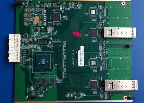
HF FR4 HASL Buried Blind Vias Multilayer PCB Assembly


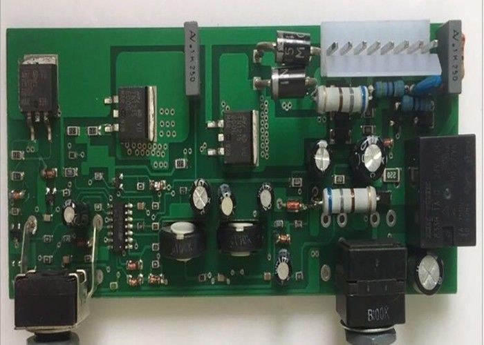
HF FR4 HASL PB FREE Buried vias Blind vias Multilayer PCB Assembly
Multilayer PCB Assembly Introduction
Haina Lean supply One-stop Fabrication and assembly service , include :SMT Assembly , BGA Assembly , Through-Hole Assembly ,Mixed Assembly,Rigid Flex PCB Assembly services . etc.
Basic Information
| Model NO. | PCBA | Condition | New |
| MOQ | 1 PCs | Layer | 1-36 Layers |
| surface Finishing | HASL. Enig, OSP, Immersion Au.AG,Sn |
Min.Hole size | 3 Mil |
| Board Thickness | 0.2mm-4mm | Min.Line Spacing | 3 Mil |
| copper Thickness | 0.5oz-6oz(18 Um-770 um) | solder Mask | Green, White,Black. Blue(Customized) |
| specialised | CE,LED.Medical, Industrial, Control Board |
service | PCB/PCBA/Circuit Board/SMT/DIP |
| other Service | PCBA Layout and Design, Engineering support |
PCBA QA | X-ray,Aoi Test, Function Test(100% Test) |
| Delivery | PCB,7-10 Days;PCBA,2- 3weeks |
specification | CE,UL,SGS,IS09001,94v0 |
| Trademark | OEM PCB Assembly PCBA | Transport Package |
Vacuum |
Multilayer PCB Assembly Craftsmanship
Immersion gold (ENIG) ,Lead-free HASL,OSP,FINGER GOLD ,Immersion Silver Ag ,Immersion Tin etc.
![]()
![]()
![]()
![]()
Our service
Electronic Manufacturing Service
Components Sourcing
Electronic Design
PCB Sourcing Service
PCB Layout Service
PCB Supplier & Quality Inspection Service
![]()
Multilayer PCB Assembly Application Field
Printed circuit boards And PCB Assembly are mainly used for many communication industry, medical equipments, consumer electronics and automobile industry etc.
Our Workshop
![]()
![]()
![]()
Partners
![]()
Common packaging
PCB: Vacuum packaging with carton box
PCBA: ESD packaging with carton box
![]()
Company Information
Haina lean Electronics Co., Ltd is a one-stop EMS supplier integrating PCB design, PCB manufacturing, Component sourcing and PCB assembly.
Our company was established in May 1, 2012 in Beijing. And expansion was completed in June 2016. The company is specialized in electronic products supporting processing services, mainly to undertake circuit board design, layout production, components procurement, PCB plate making, circuit board welding assembly debugging and other OEM/ODM services.
Our first factory is located in Changping District, Beijing, the main radiation Haidian, Changping, Chaoyang three areas of Beijing. Since our company’s establishment, we have been adhering to creating high quality, high efficiency, low-cost business philosophy based on the circuit board processing industry for customers. Most of the key staff of the company are mature technical talents who have been engaged in the industry for more than 10 years, and have rich experience in the production of SMT and DIP, also has rich experience in production for high density & difficulty to package components such as BGA. The factory covers an area of 1500 square meters. Since its establishment, we obtain a good reputation in the industry through the continuous efforts of all staff and high quality service . Our second branch plant is located in Langfang city, and mainly cover Fengtai and Daxing Yizhuang area.
At present, the main cooperation industries are automotive electronics, communications, audio and video, optoelectronics, robotics, hydroelectric power, medical care, aerospace, education, radio frequency, power supply, printer etc industries.
![]()
Our services cover all industries and reach all parts of the world.