-
High Light
OSP Contract PCB Assembly
,SMD Contract PCB Assembly
,ISO9001 SMD PCB Assembly
-
Product NameContract PCB Assembly
-
MaterialHigh Tg FR-4
-
Layers1-46layers
-
Copper Thickness0.3oz 0.6oz 1.0oz 2oz ...... 6oz
-
Min. Line Spacing / Width0.030mm / 0.030mm
-
Board Thickness0.3mm-3.5mm
-
Min. Hole SizeLaser 0.05mm ; Mechnical 0.15
-
Surface TreatmentOSP,HAL,HAL LF,ENIG,Hard Gold,Imm Ag,Imm Sn,Peelable Soldermask,Carbon Ink Print,Selective Hard Gold
-
ApplicationConsumer Electronics,Industry/Medical/Consumer Electronic,PCBA Circuit Board
-
Solder Mask ColorGreen,white,black,red,orange,yellow,blue,purple
-
Acceptable FileProtel,PADS,POWERPCB,AutoCAD,ORCAD
-
ServicePCB/PCBA/Circuit Board/SMT/DIP PCBA Layout And Design
-
Place of OriginCHINA
-
Brand NameHNL-PCBA
-
CertificationISO9001,IS16949, ISO14001,ROHS ,IPC-A ,QC080000
-
Model NumberPCB Assembly
-
Minimum Order Quantity1 PC
-
PriceNegotiable
-
Packaging DetailsESD packaging with carton box
-
Delivery Time1-7days
-
Payment TermsT/T, Western Union, L/C, MoneyGram
-
Supply Ability10,000,000 Point /Day
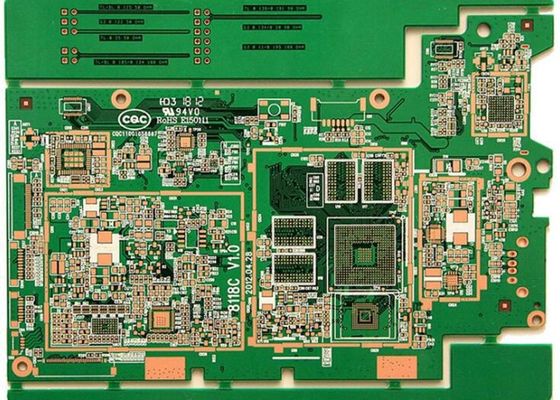
ISO9001 High Tg FR-4 OSP SMD Contract PCB Assembly

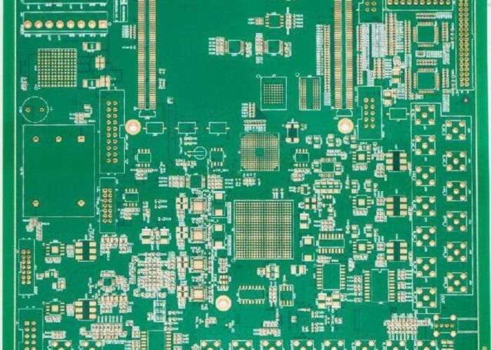
High Tg FR-4 OSP SMD Contract PCB Assembly
Contract PCB Assembly Introduction
PCBA is the abbreviation of Printed Circuit Board Assembly in English, that is to say, PCB blank board goes through SMT loading, or the entire process of DIP plug-in, referred to as PCBA, and the standard way of writing in Europe and America is PCB'A, with "'" added, this Known as the official idiom.
Factory Capacity
| Layers | 1 - 46 L |
| Substrate | FR-4,CTI600,Tg180,,Anti CAF,Halogen-free,,High frequency,Tg170&HF |
| Max. panel size | 700x610mm |
| Board thickness | 0.3 mm - 3.5 mm. |
| Copper thickness | 1/3 oz. to 6 oz. (outer) (Max) |
| Hole | > 0.15mm. |
| Aspect Ratio | 10 : 1 |
| Min. track width | 3.0 mils(partial) |
| Min. track space | 3.0mils(partial) |
| Min. S/M bridge | 3mil |
| Hole plugging diameter | 0.3 mm~0.55 mm. |
| Impedance tolerance | +/- 10%. |
| Color of S/M | green,white,black,red,orange,yellow,blue,purple |
| Surface treatment | OSP,HAL,HAL LF,ENIG,Hard gold,Imm Ag,Imm Sn,Peelable soldermask,Carbon ink print,Selective hard gold |
Our service
PCB Design & Layout
PCB Prototyping
PCB Fabrication
Turn Prototype PCB Assembly
PCB Assembly Services
PCB'A
![]()
Workshop & Equipment
AL-SPI-IA
solder paste printing equipment
wave-soldering
automatic printing equipment
60times magnifying glass
material baking equipment
X-ray welding inspection
Semi-automatic printing equipment
component counting equipment
Online AOI detector
Reflow welding equipment
Mydata welding equipment
![]()
Contract PCB Assembly Application
Aprospace ,Auto Industry ,Communication,Indutrial Control ,Medical device ,Smart Home.etc.
![]()
Common packaging
PCB: Vacuum packaging with carton box
PCBA: ESD packaging with carton box
![]()
Our services cover all industries and reach all parts of the world.