
-
High Light
SMT Lead Free PCB Assembly
,DIP Lead Free PCB Assembly
,6oz multilayer PCB assembly
-
Product NamePCBA Electronics
-
MaterialFR-4/Normal Tg/High Tg/Low Dk/HF FR4/ Aluminium
-
Layers1-36layers
-
Copper Thickness0.3oz-6oz
-
Min. Line Spacing0.030mm/0.030mm
-
Board Thickness0.3-3.5mm
-
Min. Line Width0.03mm
-
Min. Hole SizeLaser 0.05mm ; Mechnical 0.15
-
Surface FinishingHASL,OSP,ENIG,HASL Lead Free,Immersion Gold
-
Base MaterialHigh Tg FR-4, Halogen Free FR-4, Thick Copper FR-4, Aluminium Based, Rogers, Taconic
-
Solder Mask ColorGreen, Yellow, Red, Black, Blue, Whiteetc
-
Solder TypeWater Soluble Solder Paste, Leaded And Lead-Free
-
File FormateGerber Files, Pick-N-Place File, BOM ,PADs ,Protel,CAD
-
TestingFlying Probe Test,X-ray Inspection AOI Test
-
PCB Assembly ProcessDrilling--Exposure--Plating--Etaching & Stripping--Punching--Electrical Testing--SMT--Wave Soldering--Assembling-- ICT--Function Testing--Temperature & Humidity Testing
-
ApplicationTelecom Communication ; ; Automotive Industry ;Industrial Control ;Consumer Electronics Office Equipment;Household ;Aerospace; Elevator; High Speed Railway.
-
Place of OriginCHINA
-
Brand NameHNL-PCBA
-
CertificationISO9001,IS16949, ISO14001,ROHS ,IPC-A ,QC080000
-
Model NumberPCB Assembly
-
Minimum Order Quantity1 PC
-
PriceNegotiable
-
Packaging DetailsESD packaging with carton box
-
Delivery Time1-7days
-
Payment TermsT/T, Western Union, L/C, MoneyGram
-
Supply Ability10,000,000 Point /Day
SMT DIP Lead Free PCB Assembly , 6oz Multilayer PCB Assembly
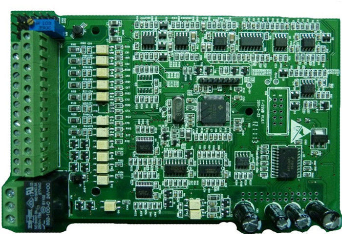
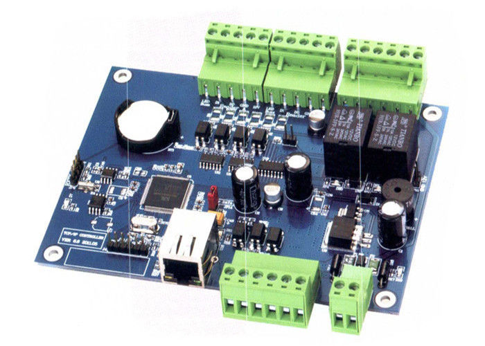
SMT DIP Process Multilayer PCBA Electronics
PCBA Electronics Introduction
PCBA refers to the complete electronic circuit board after all components have been assembled . It has many benefits that make it a much sought-after element in the communicating and electronics industry.
The PCBA is a complete assembly. You have to assemble the PCB, once it is ready. The assembling requires both passive and active components. The list of these electronic components include-
Resistor
SMD capacitor
Transformer
Diode
ICs
Transmitter
The PCBA electronic components have two types.
1. SMD components: It refers to surface mount devices. You have to use the surface mount technology to install these components on the PCB. You can identify the SMD components by measuring the number of pins in the package.
2.Through-hole components: Thru-hole or through-hole components have leads in them. The leads are inserted through the PCB board surface. You have to drill holes on the PCB surface to insert the thru-hole components into it.
There are two way to assembly of the printed circuit board . one way is You may adopt for automated soldering to mount the electronic components on the PCB. The most popular soldering technology is wave soldering. It is used for the conventional thru-hole components.
Another way widely used soldering technique for PCB components is reflow soldering . It is used for SMD components mostly. You may also use mixed soldering technology. Some expert professionals will use hand soldering too. But it is a quite difficult task.
The assembly of the PCB is completed when the electronic components are welded or assembled on the PCB.
Factory Capabilities
| PCB Assembly Capability | ||
| Item | Capability | |
| Advantages | Professional Surface-mounting and Through-hole soldering technology | |
| Various sizes like 1206,0805,0603 components SMT technology | ||
| ICT(In Circuit Test),FCT(Functional Circuit Test) | ||
| PCB Assembly With UL,ISODD,Rohs Approval | ||
| SMT process adpot reflow soldering technology | ||
| High Standard SMT & Solder Assembly Line | ||
| HDI technology (High density interconnected board placement technology capacity) | ||
| Components | Chip & IC 01005 ,55mm | |
| BGA pitch 0.3mm | ||
| QFP Pitch 0.3mm | ||
| Quantity | Prototype & Low Volume PCB Assembly,from 1 Board to 250, or up to 5000 and customized | |
| Type of Assembly | SMT, Thru-hole ,DIP ,MIX | |
| Solder Type | Water Soluble Solder Paste, Leaded and Lead-Free | |
| Bare Board Size | Largest:700X610mm | |
| File Formate | Gerber files, Pick-N-Place file, BOM ,PADs ,Protel,CAD | |
| Types of Service | Turn-key,partial turn-key or consignment | |
| Testing | Flying Probe Test,X-ray Inspection AOI Test | |
| PCB assembly process | Drilling----Exposure-----Plating-----Etaching & Stripping---Punching-----Electrical Testing-----SMT-----Wave Soldering-----Assembling---- ICT-----Function Testing-----Temperature & Humidity Testing | |
PCBA Electronics Production Process
PCB,Component sourcing ,QC ,SMT Process ,AOI ,Test ,Automatic optical inspection ,DIP Process ,Washing board ,FQC .
![]()
WorkShop
![]()
Products Show
![]()
PCBA Electronics Application Field
Aerospace ; Telecom Communication ; Automotive Industry ;Industrial Control ;Consumer Electronics .
![]()
Delivery Time
| Product Type | Qty | Normal lead time | Quick-turn lead time |
| SMT+DIP | 1-50 | 1WD-2WD | 8H |
| SMT+DIP | 51-200 | 2WD-3WD | 1.5WD |
| SMT+DIP | 201-2000 | 3WD-4WD | 2WD |
| SMT+DIP | ≥2001 | 4WD-5WD | 3WD |
| PCBA(2-4Layer) | 1-50 | 2.5WD-3.5WD | 1WD |
| PCBA(2-4Layer) | 51-2000 | 5WD-6WD | 2.5WD |
| PCBA(2-4Layer) | ≥2001 | ≥7WD | 5WD |
| PCBA(6-10Layer) | 1-50 | 3WD-4WD | 2.5WD |
| PCBA(6-10Layer) | 51-2000 | 7WD-8WD | 6WD |
| PCBA(10-HDILayer) | 1-50 | 7WD-9WD | 5WD |
| PCBA(10-HDILayer) | 51-2000 | 9WD-11WD | 7WD |
Partners
![]()
Common packaging
PCB: Vacuum packaging with carton box
PCBA: ESD packaging with carton box
![]()
Certification
![]()
FAQ
Q1:What kind of PCB file format can you accept for production?
Gerber, PROTEL 99SE, PROTEL DXP, CAM350, ODB+(.TGZ)
Q2:Is my PCB files safe when I submit them to you for manufacturing?
We respect customer's copyright and will never manufacture PCB for someone else with your files unless we receive written permission from you, nor we'll share these files with any other 3rd parties.
Q3:What payments do you accept ?
-Telex Transfer(T/T),Western Union,Letter of Credit(L/C)
-Paypal,AliPay,Credit Card
Q4:How to get the PCB?
A:For small packages, we will ship the boards to you by DHL,UPS,FedEx,EMS. Door to door service! You will get your PCBs at your home.
B:For heavy goods more than 300kg, we may ship your boards by ship or by air to save freight cost. Of course, if you have your own forwarder, we may contact them for dealing with your shipment.
Q5:What is your minimum order quantity?
Our MOQ is 1 PCS.
Q6: Can we visit your company?
No problem. You are welcome to visit us in Beijing. Or the branch factory is in Tianjin.
Q7: How can you ensure the quality of the PCB?
Our PCBs are 100% test including Flying Probe Test, E-test and AOI.
Company Information
Haina lean Electronics Co., Ltd is a one-stop EMS supplier integrating PCB design, PCB manufacturing, Component sourcing and PCB assembly.
Our company was established in May 1, 2012 in Beijing. And expansion was completed in June 2016. The company is specialized in electronic products supporting processing services, mainly to undertake circuit board design, layout production, components procurement, PCB plate making, circuit board welding assembly debugging and other OEM/ODM services.
Our first factory is located in Changping District, Beijing, the main radiation Haidian, Changping, Chaoyang three areas of Beijing. Since our company’s establishment, we have been adhering to creating high quality, high efficiency, low-cost business philosophy based on the circuit board processing industry for customers. Most of the key staff of the company are mature technical talents who have been engaged in the industry for more than 10 years, and have rich experience in the production of SMT and DIP, also has rich experience in production for high density & difficulty to package components such as BGA. The factory covers an area of 1500 square meters. Since its establishment, we obtain a good reputation in the industry through the continuous efforts of all staff and high quality service . Our second branch plant is located in Langfang city, and mainly cover Fengtai and Daxing Yizhuang area.
The company pursues "inclusiveness, excellence, people-oriented". Constantly innovate, take technology as the core, regard quality as life, and wholeheartedly provide customers with high-quality and high-efficiency humanized services.We are willing to serve our customers with the principle of continuous honesty & trustworthiness, pragmatism and innovation.
At present, the main cooperation industries are automotive electronics, communications, audio and video, optoelectronics, robotics, hydroelectric power, medical care, aerospace, education, radio frequency, power supply, printer etc industries.
![]()
Our services cover all industries and reach all parts of the world.