
-
High Light
6oz 3.5mm Printed Board Assembly
,3.5mm Printed Board Assembly
,6oz THT assembly
-
Product NameThrough Hole Printed Board Assembly
-
Layer1-36layers
-
Copper Thickness1/3oz To 6oz
-
Max Board Size700x610mm Custom
-
Min. Line Spacing / Width0.030mm /0.030mm
-
Board Thickness0.3mm 1.2mm 1.6mm , ,,,,,, 3.5mm
-
MaterialFR4 CEM1 CEM3 High TG
-
Solder MaskGreen/blue/black/red/yellow/white
-
Surface FinishingHASL,OSP,ENIG,HASL Lead Free,Immersion Gold
-
UsageCommunication Equipment, Industrial Control, Consumer Electronics, Medical Equipment, Aerospace
-
Place of OriginCHINA
-
Brand NameHNL-PCBA
-
CertificationISO9001,ISO16949, ISO14001,ROHS ,IPC-A ,QC080000
-
Model NumberPCB Assembly 02
-
Minimum Order Quantity1PC
-
PriceNegotiable
-
Packaging DetailsESD packaging with carton box
-
Delivery Time1-7days
-
Payment TermsT/T, Western Union, L/C, MoneyGram
-
Supply Ability10,000,000 Point /Day
3.5mm Through Hole Printed Board Assembly
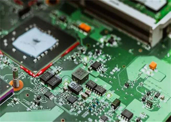
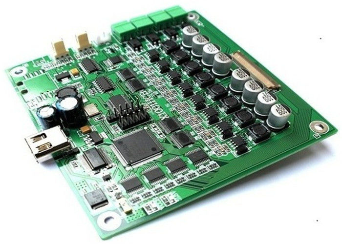
Printed Circuit Board Pcb Assembly Through Hole Printed Board Assembly
Through Hole Printed Board Assembly Introduction
Through-hole PCB assembly are the key in many mission-critical electrical assemblies.
We provide through-hole PCB assembly services to meet conventional lead assembly requirements of a variety of industries. We provide single, double-sided, as well as high-density multilayer Plated Through Hole (PTH) circuit board assembly services to meet requirements of different clients.
Haina lean Electronics is a one-stop EMS supplier integrating PCB design, PCB manufacturing, Component sourcing and PCB assembly.
The company is specialized in electronic products supporting processing services, mainly to undertake circuit board design, layout production, components procurement, PCB plate making, circuit board welding assembly debugging and other OEM/ODM services.
PCB CAPABILITIES
| FACTORY CAPABILITIES | |||
| No. | Items | 2019 | 2020 |
| 1 | HDI Capabilities | HDI ELIC (4+2+4) | HDI ELIC(5+2+5) |
| 2 | Max layer count | 32L | 36L |
| 3 | Board Thickness | Core thickness 0.05mm-1.5mm ,Fineshed board thickness 0.3-3.5mm | Core thickness 0.05mm-1.5mm ,Fineshed board thickness 0.3-3.5mm |
| 4 | Min.Hole Size | Laser 0.075mm | Laser 0.05mm |
| Mechnical 0.15mm | Mechnical 0.15mm | ||
| 5 | Min Line Width/Space | 0.035mm/0.035mm | 0.030mm/0.030mm |
| 6 | Copper Thickness | 1/3oz-4oz | 1/3oz-6oz |
| 7 | Size Max Panel size | 700x610mm | 700x610mm |
| 8 | Registration Accuracy | +/-0.05mm | +/-0.05mm |
| 9 | Routing Accuracy | +/-0.075mm | +/-0.05mm |
| 10 | Min.BGA PAD | 0.15mm | 0.125mm |
| 11 | Max Aspect Ratio | 10:1 | 10:1 |
| 12 | Bow and Twist | 0.50% | 0.50% |
| 13 | Impedance Control Tolerance | +/-8% | +/-5% |
| 14 | Daily Output | 3,000m2 (Max capacity of equipment) | 4,000m2 (Max capacity of equipment) |
| 15 | Surface Finishing | ENEPING /ENIG /HASL /FINGER GOLD/IMMERSION TIN/SELECTIVE THICK GOLD | |
| 16 | Raw Material | FR-4/Normal Tg/High Tg/Low Dk/HF FR4/PTEE/PI | |
PCBA CAPABILITIES
| PCBA Capability | |||
| Material Type | Item | Min | Max |
| PCB | Dimension (length,width,height.mm) | 50*40*0.38 | 600*400*4.2 |
| Material | FR-4,CEM-1,CEM-3,Aluminium-based board,Rogers,ceramic plate,FPC | ||
| Surface finish | HASL,OSP,Immersion gold,Flash Gold Finger | ||
| Components | Chip&IC | 1005 | 55mm |
| BGA Pitch | 0.3mm | - | |
| QFP Pitch | 0.3mm | - | |
| SMT capabilities | DIP function |
|
SMT Assembly: SMT provides a flexible high technology. These solutions include: 7 high-speed placement machines, 7 automatic printers with fiducial alignment, 2 X-ray machines, BGA maintenance machines, ICT test machines |
A-8 semi-assembly production line with four wave soldering machines 1 U-shaped automatic assembly line for box-type building products with test stations High temperature / low temperature aging test furnace B-4 for products required for aging test With time control and temperature control All products are 100% inspected and tested during the DIP process |
PCB Assembly Process
1.Solder Paste stenciling
2.Surface Mount Technology (Pick and Place)
3.Reflow Soldering
4.Inspection and Quality Control
5.Through-Hole Component Insertion (DIP Process)
6.Final Inspection and Functional Test
7.Packing
8.Shipment
![]()
Our advantage
Service value:
Independent quotation system to quickly serve the market
PCB manufacturing:
High-tech PCB and PCB assembly production line
Material purchasing:
A team of experienced electronic component procurement engineers
SMT post soldering:
Dust-free workshop, high-end SMT patch processing
![]()
![]()
Through-Hole Process PCB Assembly Application Field
Printed circuit boards And PCB Assembly are mainly used for many communication industry, medical equipments, consumer electronics ,automotive electronics , Elevator,audio and video, optoelectronics, robotics, hydroelectric power, Elevator,aerospace, education, power supply, printer ,Auto Industry ,Smart Home.etc.
![]()
Workshop
![]()
![]()
![]()
Partners
![]()
Common packaging
PCB: Vacuum packaging with carton box
PCBA: ESD packaging with carton box
![]()
FAQ
1.What are needed for quotation?
PCB: Quantity, Gerber file and Technic requirements(material,surface finish treatment, copper thickness,board thickness ......)
PCBA: PCB information, BOM, (Testing documents...)
2. What file formats do you accept for production?
Gerber file: CAM350 RS274X
PCB file: Protel 99SE, P-CAD 2001 PCB
BOM: Excel (PDF,word,txt)
3.Are my files safe?
Your files are held in complete safety and security.We protect the intellectual property for our customers in the whole process.. All documents from customers are never shared with any third party.
4.MOQ?
There is no MOQ .We can flexibly handle small and mass production.
5.Shipping Cost ?
The shipping cost is determined by the destination ,weight ,packing size of the goods .We can provide shipping, air, land, express and other transportation services .
6.How to ensure high-quality production?
The process is strictly controlled under ISO 9001:2015 standards.
Most of our advanced equipment and tools are imported from abroad. Such as Flying Probe, X-ray Inspection, AOI (Automated Optical Inspector) and ICT (in-circuit testing).
We have a very professional QC team.
Q7.What are the services you can provide ?
One-stop contract manufacturing
A:PCB Assembly;
B:PCB Design & Layout
C:PCBA programming & functional testing;
D:Electronic components purchasing service;
E:Enclosure molding & final assembly with labels,instructions,enclosure, boxes.
Q8.Whether all PCBA s will be tested before delivery ?
Yes , we will test each piece of PCBA product under your testing methods ,to ensure quality and functionality .
Q9.Do you provide OEM service ?
Yes ,we offer PCB and PCBA OEM Service , we manufacture the PCB and PCBA products to your design and requirements .
![]()
Our services cover all industries and reach all parts of the world.